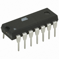
AT89LP214-20PU Atmel, AT89LP214-20PU Datasheet - Page 25

AT89LP214-20PU
Manufacturer Part Number
AT89LP214-20PU
Description
MCU 8051 2K FLASH 20MHZ 14-PDIP
Manufacturer
Atmel
Series
89LPr
Datasheet
1.AT89LP213-20PU.pdf
(98 pages)
Specifications of AT89LP214-20PU
Core Processor
8051
Core Size
8-Bit
Speed
20MHz
Connectivity
SPI, UART/USART
Peripherals
Brown-out Detect/Reset, POR, PWM, WDT
Number Of I /o
12
Program Memory Size
2KB (2K x 8)
Program Memory Type
FLASH
Ram Size
128 x 8
Voltage - Supply (vcc/vdd)
2.4 V ~ 5.5 V
Oscillator Type
Internal
Operating Temperature
-40°C ~ 85°C
Package / Case
14-DIP (0.300", 7.62mm)
Processor Series
AT89x
Core
8051
Data Bus Width
8 bit
Data Ram Size
128 B
Interface Type
SPI/UART
Maximum Clock Frequency
20 MHz
Number Of Programmable I/os
12
Number Of Timers
2
Operating Supply Voltage
2.4 V to 5 V
Maximum Operating Temperature
+ 85 C
Mounting Style
Through Hole
3rd Party Development Tools
PK51, CA51, A51, ULINK2
Development Tools By Supplier
AT89ISP
Minimum Operating Temperature
- 40 C
Lead Free Status / RoHS Status
Lead free / RoHS Compliant
Eeprom Size
-
Data Converters
-
Lead Free Status / Rohs Status
Lead free / RoHS Compliant
13.1.2
13.1.3
3538E–MICRO–11/10
Input-only Mode
Open-drain Output
Figure 13-1. Quasi-bidirectional Output
The input only port configuration is shown in
input includes a Schmitt-triggered input for improved input noise rejection. The input circuitry of
P1.3, P3.2 and P3.3 is not disabled during Power-down (see
safely driven to 5.5V even when operating at lower V
the Schmitt trigger will be set by the V
Figure 13-2. Input Only
Figure 13-3. Input Only for P1.3, P3.2 and P3.3
The open-drain output configuration turns off all pull-ups and only drives the pull-down transistor
of the port pin when the port latch contains a logic “0”. To be used as a logic output, a port con-
figured in this manner must have an external pull-up, typically a resistor tied to V
down for this mode is the same as for the quasi-bidirectional mode. The open-drain port configu-
ration is shown in
Power-down (see
operating at lower V
the V
CC
Register
From Port
level and must be taken into consideration.
Input
Input
Data
Data
Figure
Figure
CC
PWD
levels; however, the input threshold of the Schmitt trigger will be set by
13-4.The input circuitry of P1.3, P3.2 and P3.3 is not disabled during
13-3). Open-drain pins can be safely pulled high to 5.5V even when
1 Clock Delay
(D Flip-Flop)
CC
level and must be taken into consideration.
Figure
Input
Data
PWD
13-2. The output drivers are tristated. The
CC
V
Strong
levels; however, the input threshold of
CC
Port
Pin
Port
Pin
Figure
AT89LP213/214
V
Weak
Very
CC
13-3). Input pins can be
V
Weak
CC
CC
Port
Pin
. The pull-
25


