AT89LP214-20PU Atmel, AT89LP214-20PU Datasheet - Page 3
AT89LP214-20PU
Manufacturer Part Number
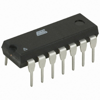
AT89LP214-20PU
Description
MCU 8051 2K FLASH 20MHZ 14-PDIP
Manufacturer
Atmel
Series
89LPr
Datasheet
1.AT89LP213-20PU.pdf
(98 pages)
Specifications of AT89LP214-20PU
Core Processor
8051
Core Size
8-Bit
Speed
20MHz
Connectivity
SPI, UART/USART
Peripherals
Brown-out Detect/Reset, POR, PWM, WDT
Number Of I /o
12
Program Memory Size
2KB (2K x 8)
Program Memory Type
FLASH
Ram Size
128 x 8
Voltage - Supply (vcc/vdd)
2.4 V ~ 5.5 V
Oscillator Type
Internal
Operating Temperature
-40°C ~ 85°C
Package / Case
14-DIP (0.300", 7.62mm)
Processor Series
AT89x
Core
8051
Data Bus Width
8 bit
Data Ram Size
128 B
Interface Type
SPI/UART
Maximum Clock Frequency
20 MHz
Number Of Programmable I/os
12
Number Of Timers
2
Operating Supply Voltage
2.4 V to 5 V
Maximum Operating Temperature
+ 85 C
Mounting Style
Through Hole
3rd Party Development Tools
PK51, CA51, A51, ULINK2
Development Tools By Supplier
AT89ISP
Minimum Operating Temperature
- 40 C
Lead Free Status / RoHS Status
Lead free / RoHS Compliant
Eeprom Size
-
Data Converters
-
Lead Free Status / Rohs Status
Lead free / RoHS Compliant


3. Pin Description
Table 3-1.
3538E–MICRO–11/10
Pin
10
11
12
13
14
1
2
3
4
5
6
7
8
9
Symbol
GND
VCC
P1.5
P1.7
P1.3
P1.2
P3.4
P3.2
P3.3
P3.5
P1.0
P1.1
P1.4
P1.6
AT89LP213 Pin Description
Type
I/O
I/O
I/O
I/O
I/O
I/O
I/O
I/O
I/O
I/O
I/O
I/O
I/O
I/O
I/O
I/O
I/O
I/O
I/O
O
O
I
I
I
I
I
I
I
I
I
I
I
I
I
I
I
I
Description
P1.5: User-configurable I/O Port 1 bit 5.
MOSI: SPI master-out/slave-in. When configured as master, this pin is an output. When configured as
slave, this pin is an input.
GPI5: General-purpose Interrupt input 5.
P1.7: User-configurable I/O Port 1 bit 7.
SCK: SPI Clock. When configured as master, this pin is an output. When configured as slave, this pin is
an input.
GPI7: General-purpose Interrupt input 7.
P1.3: User-configurable I/O Port 1 bit 3 (if Reset Fuse is disabled).
RST: External Active-Low Reset input (if Reset Fuse is enabled.
GPI3: General-purpose Interrupt input 3.
DCL: Serial Clock input for On-chip Debug Interface when OCD is enabled.
Ground
P1.2: User-configurable I/O Port 1 bit 2.
GPI2: General-purpose Interrupt input 2.
P3.4: User-configurable I/O Port 3 bit 4.
T0: Timer/Counter 0 External Input or PWM Output.
P3.2: User-configurable I/O Port 3 bit 2.
XTAL1: Input to the inverting oscillator amplifier and internal clock generation circuits. It may be used as
a port pin if the internal RC oscillator is selected as the clock source.
DDA: Serial Data input/output for On-chip Debug Interface when OCD is enabled and the internal RC
oscillator is selected as the clock source.
P3.3: User-configurable I/O Port 3 bit 3.
XTAL2: Output from inverting oscillator amplifier. It may be used as a port pin if the internal
RC oscillator is selected as the clock source.
CLKOUT: When the internal RC oscillator is selected as the clock source, may be used to output the
internal clock divided by 2.
DDA: Serial Data input/output for On-chip Debug Interface when OCD is enabled and the external
clock is selected as the clock source.
P3.5: User-configurable I/O Port 3 bit 5.
T1: Timer/Counter 1 External input or PWM output.
Supply Voltage
P1.0: User-configurable I/O Port 1 bit 0.
AIN0: Analog Comparator Positive input.
GPI0: General-purpose Interrupt input 0.
P1.1: User-configurable I/O Port 1 bit 1.
AIN1: Analog Comparator Negative input.
GPI1: General-purpose Interrupt input 1
P1.4: User-configurable I/O Port 1 bit 4.
SS: SPI slave select input.
GPI4: General-purpose Interrupt input 4.
P1.6: User-configurable I/O Port 1 bit 6.
MISO: SPI master-in/slave-out. When configured as master, this pin is an input. When configured
as slave, this pin is an output.
GPI6: General-purpose Interrupt input 6.
See “External Reset” on page
AT89LP213/214
16).
3
Related parts for AT89LP214-20PU
Image
Part Number
Description
Manufacturer
Datasheet
Request
R

Part Number:
Description:
Manufacturer:
Atmel Corporation
Datasheet:

Part Number:
Description:
MCU 8051 2K FLASH 20MHZ 14-TSSOP
Manufacturer:
Atmel
Datasheet:

Part Number:
Description:
Microcontrollers (MCU) SINGLE CYCLE 2K ISP FLASH 2.4-5.5V
Manufacturer:
Atmel
Part Number:
Description:
At89lp213 8-bit Microcontroller With 2k Bytes Flash
Manufacturer:
ATMEL Corporation
Datasheet:

Part Number:
Description:
8-bit Microcontrollers - MCU Microcontroller
Manufacturer:
Atmel

Part Number:
Description:
DEV KIT FOR AVR/AVR32
Manufacturer:
Atmel
Datasheet:
Part Number:
Description:
INTERVAL AND WIPE/WASH WIPER CONTROL IC WITH DELAY
Manufacturer:
ATMEL Corporation
Datasheet:
Part Number:
Description:
Low-Voltage Voice-Switched IC for Hands-Free Operation
Manufacturer:
ATMEL Corporation
Datasheet:
Part Number:
Description:
MONOLITHIC INTEGRATED FEATUREPHONE CIRCUIT
Manufacturer:
ATMEL Corporation
Datasheet:
Part Number:
Description:
AM-FM Receiver IC U4255BM-M
Manufacturer:
ATMEL Corporation
Datasheet:
Part Number:
Description:
Monolithic Integrated Feature Phone Circuit
Manufacturer:
ATMEL Corporation
Datasheet:
Part Number:
Description:
Multistandard Video-IF and Quasi Parallel Sound Processing
Manufacturer:
ATMEL Corporation
Datasheet: