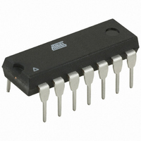
AT89LP214-20PU Atmel, AT89LP214-20PU Datasheet - Page 28

AT89LP214-20PU
Manufacturer Part Number
AT89LP214-20PU
Description
MCU 8051 2K FLASH 20MHZ 14-PDIP
Manufacturer
Atmel
Series
89LPr
Datasheet
1.AT89LP213-20PU.pdf
(98 pages)
Specifications of AT89LP214-20PU
Core Processor
8051
Core Size
8-Bit
Speed
20MHz
Connectivity
SPI, UART/USART
Peripherals
Brown-out Detect/Reset, POR, PWM, WDT
Number Of I /o
12
Program Memory Size
2KB (2K x 8)
Program Memory Type
FLASH
Ram Size
128 x 8
Voltage - Supply (vcc/vdd)
2.4 V ~ 5.5 V
Oscillator Type
Internal
Operating Temperature
-40°C ~ 85°C
Package / Case
14-DIP (0.300", 7.62mm)
Processor Series
AT89x
Core
8051
Data Bus Width
8 bit
Data Ram Size
128 B
Interface Type
SPI/UART
Maximum Clock Frequency
20 MHz
Number Of Programmable I/os
12
Number Of Timers
2
Operating Supply Voltage
2.4 V to 5 V
Maximum Operating Temperature
+ 85 C
Mounting Style
Through Hole
3rd Party Development Tools
PK51, CA51, A51, ULINK2
Development Tools By Supplier
AT89ISP
Minimum Operating Temperature
- 40 C
Lead Free Status / RoHS Status
Lead free / RoHS Compliant
Eeprom Size
-
Data Converters
-
Lead Free Status / Rohs Status
Lead free / RoHS Compliant
14. Enhanced Timer/Counters
28
AT89LP213/214
Table 13-5.
The AT89LP213/214 has two 16-bit Timer/Counter registers: Timer 0 and Timer 1. As a Timer,
the register increase every clock cycle by default. Thus, the register counts clock cycles. Since a
clock cycle consists of one oscillator period, the count rate is equal to the oscillator frequency.
The timer rate can be prescaled by a value between 1 and 16 using the Timer Prescaler (see
Table 9-2 on page
As a Counter, the register is incremented in response to a l-to-0 transition at its corresponding
input pin, T0 or T1. The external input is sampled every clock cycle. When the samples show a
high in one cycle and a low in the next cycle, the count is incremented. The new count value
appears in the register during the cycle following the one in which the transition was detected.
Since 2 clock cycles are required to recognize a l-to-0 transition, the maximum count rate is 1/2
of the oscillator frequency. There are no restrictions on the duty cycle of the input signal, but it
should be held for at least one full clock cycle to ensure that a given level is sampled at least
once before it changes. In the AT89LP214, the T0 and T1 inputs are not available at the pins.
Port Pin
P1.0
P1.1
P1.2
P1.3
P1.4
P1.5
P1.6
P1.7
P3.0
P3.1
P3.2
P3.3
P3.4
P3.5
P3.6
Port Pin Alternate Functions
PxM0.y
P1M0.0
P1M0.1
P1M0.2
P1M0.3
P1M0.4
P1M0.5
P1M0.6
P1M0.7
P3M0.0
P3M0.1
P3M0.2
P3M0.3
P3M0.4
P3M0.5
14). Both Timers share the same prescaler.
Configuration Bits
not configurable
PxM1.y
P1M1.0
P1M1.1
P1M1.2
P1M1.3
P1M1.4
P1M1.5
P1M1.6
P1M1.7
P3M1.0
P3M1.1
P3M1.2
P3M1.3
P3M1.4
P3M1.5
Alternate
CMPOUT
Function
CLKOUT
MOSI
MISO
GPI0
GPI1
GPI2
GPI3
GPI4
GPI5
GPI6
GPI7
AIN0
AIN1
RXD
INT0
INT1
SCK
TXD
SS
T0
T1
Notes
input-only
input-only
Resets to quasi-bidirectional
AT89LP214 Only
Set as output on AT89LP213
Internal RC Oscillator Only
Internal RC Oscillator or
External Clock Source Only
AT89LP213 Only
Set as output on AT89LP214
Pin is tied to comparator output
RST must be disabled
3538E–MICRO–11/10


