AT89LP214-20PU Atmel, AT89LP214-20PU Datasheet - Page 13
AT89LP214-20PU
Manufacturer Part Number
AT89LP214-20PU
Description
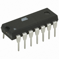
MCU 8051 2K FLASH 20MHZ 14-PDIP
Manufacturer
Atmel
Series
89LPr
Datasheet
1.AT89LP213-20PU.pdf
(98 pages)
Specifications of AT89LP214-20PU
Core Processor
8051
Core Size
8-Bit
Speed
20MHz
Connectivity
SPI, UART/USART
Peripherals
Brown-out Detect/Reset, POR, PWM, WDT
Number Of I /o
12
Program Memory Size
2KB (2K x 8)
Program Memory Type
FLASH
Ram Size
128 x 8
Voltage - Supply (vcc/vdd)
2.4 V ~ 5.5 V
Oscillator Type
Internal
Operating Temperature
-40°C ~ 85°C
Package / Case
14-DIP (0.300", 7.62mm)
Processor Series
AT89x
Core
8051
Data Bus Width
8 bit
Data Ram Size
128 B
Interface Type
SPI/UART
Maximum Clock Frequency
20 MHz
Number Of Programmable I/os
12
Number Of Timers
2
Operating Supply Voltage
2.4 V to 5 V
Maximum Operating Temperature
+ 85 C
Mounting Style
Through Hole
3rd Party Development Tools
PK51, CA51, A51, ULINK2
Development Tools By Supplier
AT89ISP
Minimum Operating Temperature
- 40 C
Lead Free Status / RoHS Status
Lead free / RoHS Compliant
Eeprom Size
-
Data Converters
-
Lead Free Status / Rohs Status
Lead free / RoHS Compliant


9.2
9.3
9.4
3538E–MICRO–11/10
External Clock Source
Internal RC Oscillator
System Clock Out
The external clock option disables the oscillator amplifier and allows XTAL1 to be driven directly
by the clock source as shown in
or configured to output a divided version of the system clock.
Figure 9-2.
The AT89LP213/214 has an internal RC oscillator tuned to 8.0 MHz ±1.0% at 5.0V and 25° C.
When enabled as the clock source, XTAL1 and XTAL2 may be used as P3.2 and P3.3 respec-
tively. XTAL2 may also be configured to output a divided version of the system clock. The
frequency of the oscillator may be adjusted by changing the RC Adjust Fuses.
figuration Fuses” on page
the Atmel SIgnature.
When the AT89LP213/214 is configured to use either an external clock or the internal RC oscil-
lator, a divided version of the system clock may be output on XTAL2 (P3.3). The Clock Out
feature is enabled by setting the COE bit in CLKREG. The two CDV bits determine the clock
divide ratio. For example, setting COE = “1” and CDIV = “00” when using the internal oscillator
will result in a 4.0 MHz clock output on P3.3. P3.3 must be configured as an output in order to
use the clock out feature.
External Clock Drive Configuration
72). A copy of the initial factory setting is stored at location 0007h of
OSCILLATOR
NC, GPIO, or
EXTERNAL
Figure
CLKOUT
SIGNAL
9-2. XTAL2 may be left unconnected, used as P3.3 I/O,
XTAL2 (P3.3)
XTAL1 (P3.2)
GND
AT89LP213/214
(See “User Con-
13
Related parts for AT89LP214-20PU
Image
Part Number
Description
Manufacturer
Datasheet
Request
R

Part Number:
Description:
Manufacturer:
Atmel Corporation
Datasheet:

Part Number:
Description:
MCU 8051 2K FLASH 20MHZ 14-TSSOP
Manufacturer:
Atmel
Datasheet:

Part Number:
Description:
Microcontrollers (MCU) SINGLE CYCLE 2K ISP FLASH 2.4-5.5V
Manufacturer:
Atmel
Part Number:
Description:
At89lp213 8-bit Microcontroller With 2k Bytes Flash
Manufacturer:
ATMEL Corporation
Datasheet:

Part Number:
Description:
8-bit Microcontrollers - MCU Microcontroller
Manufacturer:
Atmel

Part Number:
Description:
DEV KIT FOR AVR/AVR32
Manufacturer:
Atmel
Datasheet:
Part Number:
Description:
INTERVAL AND WIPE/WASH WIPER CONTROL IC WITH DELAY
Manufacturer:
ATMEL Corporation
Datasheet:
Part Number:
Description:
Low-Voltage Voice-Switched IC for Hands-Free Operation
Manufacturer:
ATMEL Corporation
Datasheet:
Part Number:
Description:
MONOLITHIC INTEGRATED FEATUREPHONE CIRCUIT
Manufacturer:
ATMEL Corporation
Datasheet:
Part Number:
Description:
AM-FM Receiver IC U4255BM-M
Manufacturer:
ATMEL Corporation
Datasheet:
Part Number:
Description:
Monolithic Integrated Feature Phone Circuit
Manufacturer:
ATMEL Corporation
Datasheet:
Part Number:
Description:
Multistandard Video-IF and Quasi Parallel Sound Processing
Manufacturer:
ATMEL Corporation
Datasheet: