MC68HC908JL8CSPE Freescale Semiconductor, MC68HC908JL8CSPE Datasheet - Page 160
MC68HC908JL8CSPE
Manufacturer Part Number
MC68HC908JL8CSPE
Description
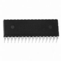
IC MCU 8K FLASH 8MHZ 32-DIP
Manufacturer
Freescale Semiconductor
Series
HC08r
Specifications of MC68HC908JL8CSPE
Core Processor
HC08
Core Size
8-Bit
Speed
8MHz
Connectivity
SCI
Peripherals
LED, LVD, POR, PWM
Number Of I /o
26
Program Memory Size
8KB (8K x 8)
Program Memory Type
FLASH
Ram Size
256 x 8
Voltage - Supply (vcc/vdd)
2.7 V ~ 5.5 V
Data Converters
A/D 13x8b
Oscillator Type
Internal
Operating Temperature
-40°C ~ 85°C
Package / Case
32-SDIP (0.400", 10.16mm)
Controller Family/series
HC08
No. Of I/o's
26
Ram Memory Size
256Byte
Cpu Speed
8MHz
No. Of Timers
2
Embedded Interface Type
I2C, SCI, SPI
Rohs Compliant
Yes
Processor Series
HC08JL
Core
HC08
Data Bus Width
8 bit
Data Ram Size
256 B
Interface Type
SCI
Maximum Clock Frequency
8 MHz
Number Of Programmable I/os
26
Number Of Timers
4
Operating Supply Voltage
0 V to 5 V
Maximum Operating Temperature
+ 125 C
Mounting Style
Through Hole
Development Tools By Supplier
FSICEBASE, DEMO908JL16E, M68CBL05CE
Minimum Operating Temperature
- 40 C
On-chip Adc
8 bit, 13 Channel
Lead Free Status / RoHS Status
Lead free / RoHS Compliant
Eeprom Size
-
Lead Free Status / Rohs Status
Details
Available stocks
Company
Part Number
Manufacturer
Quantity
Price
Company:

Part Number:
MC68HC908JL8CSPE
Manufacturer:
SINOPOWER
Quantity:
24 000
Company:
Part Number:
MC68HC908JL8CSPE
Manufacturer:
Freescale Semiconductor
Quantity:
135
Company:
Part Number:
MC68HC908JL8CSPE
Manufacturer:
FREESCALE
Quantity:
51
Part Number:
MC68HC908JL8CSPE
Manufacturer:
FREESCALE
Quantity:
20 000


Input/Output (I/O) Ports
11.4.3 Port D Control Register (PDCR)
The port D control register enables/disables the pull-up resistor and slow-edge high current capability of
pins PTD6 and PTD7.
SLOWDx — Slow Edge Enable
PTDPUx — Port D Pull-up Enable Bits
11.5 Port E
Port E is a 2-bit special function port that shares its pins with the timer 2 interface module (see
11.5.1 Port E Data Register (PTE)
The port E data register contains a data latch for each of the two port E pins.
PTE[1:0] — Port E Data Bits
160
The SLOWD6 and SLOWD7 bits enable the slow-edge, open-drain, high current output (25mA sink)
of port pins PTD6 and PTD7 respectively. DDRDx bit is not affected by SLOWDx.
The PTDPU6 and PTDPU7 bits enable the pull-up device on PTD6 and PTD7 respectively, regardless
the status of DDRDx bit.
These read/write bits are software programmable. Data direction of each port E pin is under the control
of the corresponding bit in data direction register E. Reset has no effect on port D data.
1 = Slow edge enabled; pin is open-drain output
0 = Slow edge disabled; pin is push-pull (standard I/O)
1 = Enable pull-up device
0 = Disable pull-up device
Alternative Functions:
Address:
Reset:
Read:
Write:
MC68HC908JL8/JK8 • MC68HC08JL8/JK8 • MC68HC908KL8 Data Sheet, Rev. 3.1
Address:
Reset:
Read:
Write:
$000A
Bit 7
0
0
PTE0–PTE1 are available on 32-pin packages only.
Figure 11-13. Port D Control Register (PDCR)
$0008
Bit 7
Figure 11-14. Port E Data Register (PTE)
6
0
0
6
5
0
0
5
NOTE
4
0
0
Unaffected by reset
4
SLOWD7
3
0
3
SLOWD6
2
0
2
PTDPU7
1
0
T2CH1
PTE1
1
Freescale Semiconductor
PTDPU6
Bit 0
0
T2CH0
PTE0
Bit 0
Chapter
8).
Related parts for MC68HC908JL8CSPE
Image
Part Number
Description
Manufacturer
Datasheet
Request
R

Part Number:
Description:
Manufacturer:
Freescale Semiconductor, Inc
Datasheet:
Part Number:
Description:
Manufacturer:
Freescale Semiconductor, Inc
Datasheet:
Part Number:
Description:
Manufacturer:
Freescale Semiconductor, Inc
Datasheet:
Part Number:
Description:
Manufacturer:
Freescale Semiconductor, Inc
Datasheet:
Part Number:
Description:
Manufacturer:
Freescale Semiconductor, Inc
Datasheet:
Part Number:
Description:
Manufacturer:
Freescale Semiconductor, Inc
Datasheet:
Part Number:
Description:
Manufacturer:
Freescale Semiconductor, Inc
Datasheet:
Part Number:
Description:
Manufacturer:
Freescale Semiconductor, Inc
Datasheet:
Part Number:
Description:
Manufacturer:
Freescale Semiconductor, Inc
Datasheet:
Part Number:
Description:
Manufacturer:
Freescale Semiconductor, Inc
Datasheet:
Part Number:
Description:
Manufacturer:
Freescale Semiconductor, Inc
Datasheet:
Part Number:
Description:
Manufacturer:
Freescale Semiconductor, Inc
Datasheet:
Part Number:
Description:
Manufacturer:
Freescale Semiconductor, Inc
Datasheet:
Part Number:
Description:
Manufacturer:
Freescale Semiconductor, Inc
Datasheet:
Part Number:
Description:
Manufacturer:
Freescale Semiconductor, Inc
Datasheet: