MC68HC908JL8CSPE Freescale Semiconductor, MC68HC908JL8CSPE Datasheet
MC68HC908JL8CSPE
Specifications of MC68HC908JL8CSPE
Available stocks


Related parts for MC68HC908JL8CSPE

MC68HC908JL8CSPE Summary of contents
Page 1
MC68HC908JL8 MC68HC908JK8 MC68HC908KL8 MC68HC08JL8 MC68HC08JK8 Data Sheet M68HC08 Microcontrollers MC68HC908JL8 Rev. 3.1 3/2005 freescale.com ...
Page 2
...
Page 3
... The following revision history table summarizes changes contained in this document. For your convenience, the page number designators have been linked to the appropriate location. Freescale™ and the Freescale logo are trademarks of Freescale Semiconductor, Inc. This product incorporates SuperFlash® technology licensed from SST. ...
Page 4
... MC68HC908JL8/JK8 • MC68HC08JL8/JK8 • MC68HC908KL8 Data Sheet, Rev. 3.1 4 Description Table 17-5 . Control Timing (5V) — STOP_ICLKDIS bit does not affect stop mode Appendix A MC68HC08JL8 — ROM parts. Appendix B MC68HC908KL8. Page Number(s) and Table 17-8 . 188, 190 — Corrected SCI 121–206 — 168 176 201 207 — Freescale Semiconductor ...
Page 5
... Chapter 14 Computer Operating Properly (COP 173 Chapter 15 Low Voltage Inhibit (LVI 177 Chapter 16 Break Module (BREAK 179 Chapter 17 Electrical Specifications . . . . . . . . . . . . . . . . . . . . . . . . . . . . . . . . . . . . . . . . . . 185 Chapter 18 Mechanical Specifications . . . . . . . . . . . . . . . . . . . . . . . . . . . . . . . . . . . . . . . . 195 Chapter 19 Ordering Information 199 Appendix A MC68HC08JL8 . . . . . . . . . . . . . . . . . . . . . . . . . . . . . . . . . . . . . . . . . . . . . . . . . 201 Appendix B MC68HC908KL8 . . . . . . . . . . . . . . . . . . . . . . . . . . . . . . . . . . . . . . . . . . . . . . . . 207 MC68HC908JL8/JK8 • MC68HC08JL8/JK8 • MC68HC908KL8 Data Sheet, Rev. 3.1 Freescale Semiconductor 5 ...
Page 6
... List of Chapters MC68HC908JL8/JK8 • MC68HC08JL8/JK8 • MC68HC908KL8 Data Sheet, Rev. 3.1 6 Freescale Semiconductor ...
Page 7
... Mask Option Register (MOR 4.1 Introduction . . . . . . . . . . . . . . . . . . . . . . . . . . . . . . . . . . . . . . . . . . . . . . . . . . . . . . . . . . . . . . . . 45 4.2 Features 4.3 CPU Registers . . . . . . . . . . . . . . . . . . . . . . . . . . . . . . . . . . . . . . . . . . . . . . . . . . . . . . . . . . . . . . 46 4.3.1 Accumulator . . . . . . . . . . . . . . . . . . . . . . . . . . . . . . . . . . . . . . . . . . . . . . . . . . . . . . . . . . . . . 46 4.3.2 Index Register . . . . . . . . . . . . . . . . . . . . . . . . . . . . . . . . . . . . . . . . . . . . . . . . . . . . . . . . . . . 46 4.3.3 Stack Pointer . . . . . . . . . . . . . . . . . . . . . . . . . . . . . . . . . . . . . . . . . . . . . . . . . . . . . . . . . . . . 47 MC68HC908JL8/JK8 • MC68HC08JL8/JK8 • MC68HC908KL8 Data Sheet, Rev. 3.1 Freescale Semiconductor Chapter 1 General Description Chapter 2 Memory Chapter 3 Chapter 4 Central Processor Unit (CPU) 7 ...
Page 8
... Wait Mode . . . . . . . . . . . . . . . . . . . . . . . . . . . . . . . . . . . . . . . . . . . . . . . . . . . . . . . . . . . . . . 73 5.6.2 Stop Mode . . . . . . . . . . . . . . . . . . . . . . . . . . . . . . . . . . . . . . . . . . . . . . . . . . . . . . . . . . . . . . 74 5.7 SIM Registers . . . . . . . . . . . . . . . . . . . . . . . . . . . . . . . . . . . . . . . . . . . . . . . . . . . . . . . . . . . . . . 75 5.7.1 Break Status Register (BSR 5.7.2 Reset Status Register (RSR 5.7.3 Break Flag Control Register (BFCR MC68HC908JL8/JK8 • MC68HC08JL8/JK8 • MC68HC908KL8 Data Sheet, Rev. 3.1 8 Chapter 5 System Integration Module (SIM) Freescale Semiconductor ...
Page 9
... Security . . . . . . . . . . . . . . . . . . . . . . . . . . . . . . . . . . . . . . . . . . . . . . . . . . . . . . . . . . . . . . . . . . . 93 7.5 ROM-Resident Routines . . . . . . . . . . . . . . . . . . . . . . . . . . . . . . . . . . . . . . . . . . . . . . . . . . . . . . 94 7.5.1 PRGRNGE . . . . . . . . . . . . . . . . . . . . . . . . . . . . . . . . . . . . . . . . . . . . . . . . . . . . . . . . . . . . . . 96 7.5.2 ERARNGE . . . . . . . . . . . . . . . . . . . . . . . . . . . . . . . . . . . . . . . . . . . . . . . . . . . . . . . . . . . . . . 97 7.5.3 LDRNGE . . . . . . . . . . . . . . . . . . . . . . . . . . . . . . . . . . . . . . . . . . . . . . . . . . . . . . . . . . . . . . . 98 7.5.4 MON_PRGRNGE 7.5.5 MON_ERARNGE . . . . . . . . . . . . . . . . . . . . . . . . . . . . . . . . . . . . . . . . . . . . . . . . . . . . . . . . . 99 7.5.6 MON_LDRNGE . . . . . . . . . . . . . . . . . . . . . . . . . . . . . . . . . . . . . . . . . . . . . . . . . . . . . . . . . 100 7.5.7 EE_WRITE 100 7.5.8 EE_READ . . . . . . . . . . . . . . . . . . . . . . . . . . . . . . . . . . . . . . . . . . . . . . . . . . . . . . . . . . . . . 103 MC68HC908JL8/JK8 • MC68HC08JL8/JK8 • MC68HC908KL8 Data Sheet, Rev. 3.1 Freescale Semiconductor Chapter 6 Oscillator (OSC) Chapter 7 Monitor ROM (MON) 9 ...
Page 10
... Break Characters . . . . . . . . . . . . . . . . . . . . . . . . . . . . . . . . . . . . . . . . . . . . . . . . . . . . . . 125 9.4.2.4 Idle Characters . . . . . . . . . . . . . . . . . . . . . . . . . . . . . . . . . . . . . . . . . . . . . . . . . . . . . . . . 125 9.4.2.5 Inversion of Transmitted Output . . . . . . . . . . . . . . . . . . . . . . . . . . . . . . . . . . . . . . . . . . . 126 9.4.2.6 Transmitter Interrupts . . . . . . . . . . . . . . . . . . . . . . . . . . . . . . . . . . . . . . . . . . . . . . . . . . . 126 9.4.3 Receiver . . . . . . . . . . . . . . . . . . . . . . . . . . . . . . . . . . . . . . . . . . . . . . . . . . . . . . . . . . . . . . . 126 9.4.3.1 Character Length . . . . . . . . . . . . . . . . . . . . . . . . . . . . . . . . . . . . . . . . . . . . . . . . . . . . . . 126 MC68HC908JL8/JK8 • MC68HC08JL8/JK8 • MC68HC908KL8 Data Sheet, Rev. 3.1 10 Chapter 8 Timer Interface Module (TIM) Chapter 9 Freescale Semiconductor ...
Page 11
... ADC Voltage In (ADCVIN 148 10.7 I/O Registers . . . . . . . . . . . . . . . . . . . . . . . . . . . . . . . . . . . . . . . . . . . . . . . . . . . . . . . . . . . . . . 148 10.7.1 ADC Status and Control Register . . . . . . . . . . . . . . . . . . . . . . . . . . . . . . . . . . . . . . . . . . . 148 10.7.2 ADC Data Register 150 10.7.3 ADC Input Clock Register . . . . . . . . . . . . . . . . . . . . . . . . . . . . . . . . . . . . . . . . . . . . . . . . . 150 MC68HC908JL8/JK8 • MC68HC08JL8/JK8 • MC68HC908KL8 Data Sheet, Rev. 3.1 Freescale Semiconductor Chapter 10 Analog-to-Digital Converter (ADC) 11 ...
Page 12
... Keyboard Module During Break Interrupts 171 14.1 Introduction . . . . . . . . . . . . . . . . . . . . . . . . . . . . . . . . . . . . . . . . . . . . . . . . . . . . . . . . . . . . . . . 173 14.2 Functional Description . . . . . . . . . . . . . . . . . . . . . . . . . . . . . . . . . . . . . . . . . . . . . . . . . . . . . . . 173 MC68HC908JL8/JK8 • MC68HC08JL8/JK8 • MC68HC908KL8 Data Sheet, Rev. 3.1 12 Chapter 11 Input/Output (I/O) Ports Chapter 12 External Interrupt (IRQ) Chapter 13 Keyboard Interrupt Module (KBI) Chapter 14 Computer Operating Properly (COP) Freescale Semiconductor ...
Page 13
... Break Status Register . . . . . . . . . . . . . . . . . . . . . . . . . . . . . . . . . . . . . . . . . . . . . . . . . . . . 182 16.4.4 Break Flag Control Register (BFCR 183 16.5 Low-Power Modes . . . . . . . . . . . . . . . . . . . . . . . . . . . . . . . . . . . . . . . . . . . . . . . . . . . . . . . . . . 183 16.5.1 Wait Mode . . . . . . . . . . . . . . . . . . . . . . . . . . . . . . . . . . . . . . . . . . . . . . . . . . . . . . . . . . . . . 183 16.5.2 Stop Mode . . . . . . . . . . . . . . . . . . . . . . . . . . . . . . . . . . . . . . . . . . . . . . . . . . . . . . . . . . . . . 183 MC68HC908JL8/JK8 • MC68HC08JL8/JK8 • MC68HC908KL8 Data Sheet, Rev. 3.1 Freescale Semiconductor Chapter 15 Low Voltage Inhibit (LVI) Chapter 16 Break Module (BREAK) 13 ...
Page 14
... Monitor ROM . . . . . . . . . . . . . . . . . . . . . . . . . . . . . . . . . . . . . . . . . . . . . . . . . . . . . . . . . . . . . . 204 A.7 Electrical Specifications . . . . . . . . . . . . . . . . . . . . . . . . . . . . . . . . . . . . . . . . . . . . . . . . . . . . . . 204 A.7.1 DC Electrical Characteristics 204 A.8 Memory Characteristics . . . . . . . . . . . . . . . . . . . . . . . . . . . . . . . . . . . . . . . . . . . . . . . . . . . . . . 205 A.9 MC68HC08JL8 Order Numbers 206 MC68HC908JL8/JK8 • MC68HC08JL8/JK8 • MC68HC908KL8 Data Sheet, Rev. 3.1 14 Chapter 17 Electrical Specifications Chapter 18 Mechanical Specifications Chapter 19 Ordering Information Appendix A MC68HC08JL8 Freescale Semiconductor ...
Page 15
... B.1 Introduction . . . . . . . . . . . . . . . . . . . . . . . . . . . . . . . . . . . . . . . . . . . . . . . . . . . . . . . . . . . . . . . 207 B.2 MCU Block Diagram . . . . . . . . . . . . . . . . . . . . . . . . . . . . . . . . . . . . . . . . . . . . . . . . . . . . . . . . 207 B.3 Pin Assignments . . . . . . . . . . . . . . . . . . . . . . . . . . . . . . . . . . . . . . . . . . . . . . . . . . . . . . . . . . . 207 B.4 Reserved Registers . . . . . . . . . . . . . . . . . . . . . . . . . . . . . . . . . . . . . . . . . . . . . . . . . . . . . . . . . 210 B.5 Reserved Vectors . . . . . . . . . . . . . . . . . . . . . . . . . . . . . . . . . . . . . . . . . . . . . . . . . . . . . . . . . . 210 B.6 MC68HC908KL8 Order Numbers . . . . . . . . . . . . . . . . . . . . . . . . . . . . . . . . . . . . . . . . . . . . . . 210 MC68HC908JL8/JK8 • MC68HC08JL8/JK8 • MC68HC908KL8 Data Sheet, Rev. 3.1 Freescale Semiconductor Appendix B MC68HC908KL8 15 ...
Page 16
... Table of Contents MC68HC908JL8/JK8 • MC68HC08JL8/JK8 • MC68HC908KL8 Data Sheet, Rev. 3.1 16 Freescale Semiconductor ...
Page 17
... No security feature is absolutely secure. However, Motorola’s strategy is to make reading or copying the FLASH difficult for unauthorized users. MC68HC908JL8/JK8 • MC68HC08JL8/JK8 • MC68HC908KL8 Data Sheet, Rev. 3.1 Freescale Semiconductor Table 1-1. Summary of Devices Description FLASH part ...
Page 18
... Fast 16/8 divide instruction • Binary-coded decimal (BCD) instructions • Optimization for controller applications • Efficient C language support 1.3 MCU Block Diagram Figure 1-1 shows the structure of the MC68HC908JL8. MC68HC908JL8/JK8 • MC68HC08JL8/JK8 • MC68HC908KL8 Data Sheet, Rev. 3.1 18 Freescale Semiconductor ...
Page 19
... EXTERNAL INTERRUPT * IRQ MODULE VDD POWER VSS ADC REFERENCE Figure 1-1. MC68HC908JL8 Block Diagram MC68HC908JL8/JK8 • MC68HC08JL8/JK8 • MC68HC908KL8 Data Sheet, Rev. 3.1 Freescale Semiconductor INTERNAL BUS KEYBOARD INTERRUPT MODULE 8-BIT ANALOG-TO-DIGITAL CONVERTER MODULE 2-CHANNEL TIMER INTERFACE MODULE 1 2-CHANNEL TIMER INTERFACE ...
Page 20
... PTD6/TxD 14 19 PTE0/T2CH0 15 18 PTE1/T2CH1 16 17 Figure 1-3. 32-Pin SDIP Pin Assignment PTD5/T1CH1 24 PTD2/ADC9 23 PTA4/KBI4 22 PTD3/ADC8 21 20 PTB0/ADC0 PTB1/ADC1 19 18 PTD1/ADC10 PTB2/ADC2 17 ADC12/T2CLK PTA7/KBI7 RST PTA5/KBI5 PTD4/T1CH0 PTD5/T1CH1 PTD2/ADC9 PTA4/KBI4 PTD3/ADC8 PTB0/ADC0 PTB1/ADC1 PTD1/ADC10 PTB2/ADC2 PTB3/ADC3 PTD0/ADC11 PTB4/ADC4 Freescale Semiconductor ...
Page 21
... PTB7/ADC7 PTB6/ADC6 PTB5/ADC5 PTD7/RxD PTD6/TxD The 20-pin MC68HC908JL8 is designated MC68HC908JK8. Figure 1-5. 20-Pin PDIP/SOIC Pin Assignment 1.5 Pin Functions Description of the pin functions are provided in MC68HC908JL8/JK8 • MC68HC08JL8/JK8 • MC68HC908KL8 Data Sheet, Rev. 3.1 Freescale Semiconductor 28 1 RST 2 27 PTA5/KBI5 26 PTD4/T1CH0 3 ...
Page 22
... TST In VDD Out VDD Out VDD In/Out VDD In VSS to VDD In VDD In/Out VDD In VDD In VDD Out VSS Out VDD In/Out VDD In VSS to VDD In/Out VDD Input VSS to VDD Out VSS In/Out VDD In/Out VDD Out VSS Out VDD In VDD Freescale Semiconductor ...
Page 23
... PTA7/KBI7, PTE0/T2CH0, PTE1/T2CH1, and ADC12/T2CLK. Devices in 20-pin packages, the following pins are not available: PTA0/KBI0–PTA5/KBI5, PTD0/ADC11, PTD1/ADC10, PTA7/KBI7, PTE0/T2CH0, PTE1/T2CH1, and ADC12/T2CLK. MC68HC908JL8/JK8 • MC68HC08JL8/JK8 • MC68HC908KL8 Data Sheet, Rev. 3.1 Freescale Semiconductor Table 1-2. Pin Functions (Continued) PIN DESCRIPTION NOTE Pin Functions ...
Page 24
... General Description MC68HC908JL8/JK8 • MC68HC08JL8/JK8 • MC68HC908KL8 Data Sheet, Rev. 3.1 24 Freescale Semiconductor ...
Page 25
... The 959 bytes at addresses $FC00–$FDFF and $FE10–$FFCE are reserved ROM addresses that contain the instructions for the monitor functions. (See MC68HC908JL8/JK8 • MC68HC08JL8/JK8 • MC68HC908KL8 Data Sheet, Rev. 3.1 Freescale Semiconductor Figure 2-2, contain most of the control, status, and data registers. ...
Page 26
... BREAK ADDRESS HIGH REGISTER (BRKH) BREAK ADDRESS LOW REGISTER (BRKL) BREAK STATUS AND CONTROL REGISTER (BRKSCR) RESERVED MONITOR ROM 447 BYTES FLASH BLOCK PROTECT REGISTER (FLBPR) MASK OPTION REGISTER (MOR) RESERVED 11 BYTES USER FLASH VECTORS 36 BYTES Figure 2-1. Memory Map Freescale Semiconductor ...
Page 27
... Write: $000E (PTA7PUE) Reset: Read: $000F ↓ Unimplemented Write: $0012 U = Unaffected Figure 2-2. Control, Status, and Data Registers (Sheet MC68HC908JL8/JK8 • MC68HC08JL8/JK8 • MC68HC908KL8 Data Sheet, Rev. 3.1 Freescale Semiconductor Bit PTA7 PTA6 PTA5 PTA4 Unaffected by reset PTB7 PTB6 PTB5 PTB4 ...
Page 28
... TE RE RWU SBK ORIE NEIE FEIE PEIE BKF RPF SCR2 SCR1 SCR0 KEYF 0 IMASKK MODEK ACKK KBIE3 KBIE2 KBIE1 KBIE0 IRQF 0 IMASK MODE ACK STOP_ LVIT0 R R ICLKDIS SSREC STOP COPD PS2 PS1 PS0 Bit11 Bit10 Bit9 Bit8 Reserved Freescale Semiconductor ...
Page 29
... Write: $0033 (T2MODH) Reset: Read: TIM2 Counter Modulo $0034 Register Low Write: (T2MODL) Reset Unaffected Figure 2-2. Control, Status, and Data Registers (Sheet MC68HC908JL8/JK8 • MC68HC08JL8/JK8 • MC68HC908KL8 Data Sheet, Rev. 3.1 Freescale Semiconductor Bit Bit7 Bit6 Bit5 Bit4 Bit15 Bit14 ...
Page 30
... ELS0B ELS0A TOV0 CH0MAX Bit11 Bit10 Bit9 Bit8 Bit3 Bit2 Bit1 Bit0 ELS1B ELS1A TOV1 CH1MAX Bit11 Bit10 Bit9 Bit8 Bit3 Bit2 Bit1 Bit0 ADCH3 ADCH2 ADCH1 ADCH0 AD3 AD2 AD1 AD0 SBSW See note 0 ILAD MODRST LVI Reserved Freescale Semiconductor ...
Page 31
... Write: # (MOR) Reset: # Non-volatile FLASH registers; write by programming. Read: COP Control Register $FFFF Write: (COPCTL) Reset Unaffected Figure 2-2. Control, Status, and Data Registers (Sheet MC68HC908JL8/JK8 • MC68HC08JL8/JK8 • MC68HC908KL8 Data Sheet, Rev. 3.1 Freescale Semiconductor Bit IF6 IF5 IF4 IF3 ...
Page 32
... TIM1 Channel 0 Vector (High) IF3 $FFF7 TIM1 Channel 0 Vector (Low) IF2 — Not Used $FFFA IRQ Vector (High) IF1 $FFFB IRQ Vector (Low) $FFFC SWI Vector (High) — $FFFD SWI Vector (Low) $FFFE Reset Vector (High) — $FFFF Reset Vector (Low) Vector Freescale Semiconductor ...
Page 33
... A security feature prevents viewing of the FLASH contents security feature is absolutely secure. However, Motorola’s strategy is to make reading or copying the FLASH difficult for unauthorized users. MC68HC908JL8/JK8 • MC68HC08JL8/JK8 • MC68HC908KL8 Data Sheet, Rev. 3.1 Freescale Semiconductor Random-Access Memory (RAM) NOTE NOTE ...
Page 34
... Write any data to any FLASH address within the page address range desired. 4. Wait for a time, t (10µs). nvs 5. Set the HVEN bit. 6. Wait for a time t (4ms). erase MC68HC908JL8/JK8 • MC68HC08JL8/JK8 • MC68HC908KL8 Data Sheet, Rev. 3 HVEN Bit 0 MASS ERASE PGM Freescale Semiconductor ...
Page 35
... Write any data to any FLASH location within the address range of the row to be programmed. 4. Wait for a time, t (10µs). nvs 5. Set the HVEN bit. 6. Wait for a time, t (5µs). pgs 7. Write data to the FLASH address to be programmed. MC68HC908JL8/JK8 • MC68HC08JL8/JK8 • MC68HC908KL8 Data Sheet, Rev. 3.1 Freescale Semiconductor FLASH Mass Erase Operation NOTE NOTE 35 ...
Page 36
... Programming and erasing of FLASH locations cannot be performed by code being executed from the FLASH memory. While these operations must be performed in the order shown, other unrelated operations may occur between the steps. MC68HC908JL8/JK8 • MC68HC08JL8/JK8 • MC68HC908KL8 Data Sheet, Rev. 3.1 36 NOTE NOTE Freescale Semiconductor ...
Page 37
... This row program algorithm assumes the row programmed are initially erased. Figure 2-4. FLASH Programming Flowchart MC68HC908JL8/JK8 • MC68HC08JL8/JK8 • MC68HC908KL8 Data Sheet, Rev. 3.1 Freescale Semiconductor 1 Set PGM bit 2 Read the FLASH block protect register 3 Write any data to any FLASH location ...
Page 38
... Start address of FLASH block protect MC68HC908JL8/JK8 • MC68HC08JL8/JK8 • MC68HC908KL8 Data Sheet, Rev. 3.1 38 NOTE TST BPR6 BPR5 BPR4 BPR3 Unaffected by reset; $FF when blank 16-bit memory address 1 1 BPR[7:0] , present on the IRQ pin. This voltage 2 1 Bit 0 BPR2 BPR1 BPR0 Freescale Semiconductor ...
Page 39
... The end address of the protected range is always $FFFF. MC68HC908JL8/JK8 • MC68HC08JL8/JK8 • MC68HC908KL8 Data Sheet, Rev. 3.1 Freescale Semiconductor Start of Address of Protect Range The entire FLASH memory is protected. $DC40 (1101 1100 0100 0000) $DC80 (1101 1100 1000 0000) ...
Page 40
... Memory MC68HC908JL8/JK8 • MC68HC08JL8/JK8 • MC68HC908KL8 Data Sheet, Rev. 3.1 40 Freescale Semiconductor ...
Page 41
... The mask option register (MOR) is used to select the oscillator option for the MCU: crystal oscillator or RC oscillator. The MOR is implemented as a byte in FLASH memory. Hence, writing to the MOR requires programming the byte. MC68HC908JL8/JK8 • MC68HC08JL8/JK8 • MC68HC908KL8 Data Sheet, Rev. 3.1 Freescale Semiconductor – ...
Page 42
... COPD disables the COP module. Reset clears COPD. (See Chapter 14 Computer Operating Properly 1 = COP module disabled 0 = COP module enabled MC68HC908JL8/JK8 • MC68HC08JL8/JK8 • MC68HC908KL8 Data Sheet, Rev. 3 LVID Reserved (COP).) 13 4 – ICLK cycles 18 4 – ICLK cycles (LVI).) NOTE (COP).) 2 1 Bit 0 SSREC STOP COPD Freescale Semiconductor ...
Page 43
... OSCSEL — Oscillator Select Bit OSCSEL selects the oscillator type for the MCU. The erased or unprogrammed state of this bit is logic 1, selecting the crystal oscillator option. This bit is unaffected by reset Crystal oscillator oscillator MC68HC908JL8/JK8 • MC68HC08JL8/JK8 • MC68HC908KL8 Data Sheet, Rev. 3.1 Freescale Semiconductor ...
Page 44
... Configuration and Mask Option Registers (CONFIG & MOR) Bits 6–0 — Should be left as logic 1’s. When Crystal oscillator is selected, the OSC2/RCCLK/PTA6/KBI6 pin is used as OSC2; other functions such as PTA6/KBI6 will not be available. MC68HC908JL8/JK8 • MC68HC08JL8/JK8 • MC68HC908KL8 Data Sheet, Rev. 3.1 44 NOTE Freescale Semiconductor ...
Page 45
... Fast 8-Bit by 8-Bit Multiply and 16-Bit by 8-Bit Divide Instructions • Enhanced Binary-Coded Decimal (BCD) Data Handling • Modular Architecture with Expandable Internal Bus Definition for Extension of Addressing Range beyond 64 Kbytes • Low-Power Stop and Wait Modes MC68HC908JL8/JK8 • MC68HC08JL8/JK8 • MC68HC908KL8 Data Sheet, Rev. 3.1 Freescale Semiconductor 45 ...
Page 46
... ACCUMULATOR ( INDEX REGISTER (H:X) 0 STACK POINTER (SP) 0 PROGRAM COUNTER (PC CONDITION CODE REGISTER (CCR) CARRY/BORROW FLAG ZERO FLAG NEGATIVE FLAG INTERRUPT MASK HALF-CARRY FLAG TWO’S COMPLEMENT OVERFLOW FLAG Figure 4-1. CPU Registers Unaffected by reset Figure 4-2. Accumulator ( Bit 0 Freescale Semiconductor ...
Page 47
... During reset, the program counter is loaded with the reset vector address located at $FFFE and $FFFF. The vector address is the address of the first instruction to be executed after exiting the reset state. MC68HC908JL8/JK8 • MC68HC08JL8/JK8 • MC68HC908KL8 Data Sheet, Rev. 3.1 Freescale Semiconductor 13 12 ...
Page 48
... If the interrupt service routine modifies H, then the user must stack and unstack H using the PSHH and PULH instructions. MC68HC908JL8/JK8 • MC68HC08JL8/JK8 • MC68HC908KL8 Data Sheet, Rev. 3 Loaded with Vector from $FFFE and $FFFF Figure 4-5. Program Counter (PC NOTE Bit Bit Freescale Semiconductor ...
Page 49
... I bit remains clear. After exit by reset, the I bit is set. • Disables the CPU clock After exiting stop mode, the CPU clock begins running after the oscillator stabilization delay. MC68HC908JL8/JK8 • MC68HC08JL8/JK8 • MC68HC908KL8 Data Sheet, Rev. 3.1 Freescale Semiconductor Arithmetic/Logic Unit (ALU) 49 ...
Page 50
... B9 dd EXT IX2 – IX1 SP1 9EE9 ff SP2 9ED9 ee ff IMM AB ii DIR BB dd EXT IX2 – IX1 SP1 9EEB ff SP2 9EDB ee ff – – – – – – IMM A7 ii – – – – – – IMM AF ii Freescale Semiconductor ...
Page 51
... BHI rel Branch if Higher Branch if Higher or Same BHS rel (Same as BCC) BIH rel Branch if IRQ Pin High BIL rel Branch if IRQ Pin Low MC68HC908JL8/JK8 • MC68HC08JL8/JK8 • MC68HC908KL8 Data Sheet, Rev. 3.1 Freescale Semiconductor Table 4-1. Instruction Set Summary Description A ← (A) & ( ← ...
Page 52
... DIR (b5 DIR (b6 DIR (b7 – – – – – – REL 21 rr DIR (b0 DIR (b1 DIR (b2 DIR (b3 – – – – – DIR (b4 DIR (b5 DIR (b6 DIR (b7 DIR (b0 DIR (b1 DIR (b2 DIR (b3 – – – – – – DIR (b4 DIR (b5 DIR (b6 DIR (b7 Freescale Semiconductor ...
Page 53
... CPX opr,X CPX opr,X CPX opr,SP CPX opr,SP DAA Decimal Adjust A MC68HC908JL8/JK8 • MC68HC08JL8/JK8 • MC68HC908KL8 Data Sheet, Rev. 3.1 Freescale Semiconductor Table 4-1. Instruction Set Summary Description PC ← (PC push (PCL) SP ← (SP) – 1; push (PCH) SP ← (SP) – ← (PC) + rel PC ← (PC rel ? (A) – (M) = $00 PC ← ...
Page 54
... IX2 IX1 DIR BD dd EXT – – – – – – IX2 IX1 IMM A6 ii DIR B6 dd EXT IX2 – – – IX1 SP1 9EE6 ff SP2 9ED6 ee ff IMM – – – DIR 55 dd Freescale Semiconductor ...
Page 55
... ORA opr,X ORA ,X ORA opr,SP ORA opr,SP PSHA Push A onto Stack PSHH Push H onto Stack PSHX Push X onto Stack PULA Pull A from Stack MC68HC908JL8/JK8 • MC68HC08JL8/JK8 • MC68HC908KL8 Data Sheet, Rev. 3.1 Freescale Semiconductor Table 4-1. Instruction Set Summary Description X ← ( ← (M) ...
Page 56
... SP2 9ED2 ee ff – – – – – 1 INH 99 – – 1 – – – INH 9B DIR B7 dd EXT IX2 – – – IX1 SP1 9EE7 ff SP2 9ED7 – – – DIR 35 dd – – 0 – – – INH 8E Freescale Semiconductor ...
Page 57
... TST opr,SP TSX Transfer SP to H:X TXA Transfer TXS Transfer H MC68HC908JL8/JK8 • MC68HC08JL8/JK8 • MC68HC908KL8 Data Sheet, Rev. 3.1 Freescale Semiconductor Table 4-1. Instruction Set Summary Description M ← (X) A ← (A) – (M) PC ← (PC Push (PCL) SP ← (SP) – 1; Push (PCH) SP ← (SP) – 1; Push (X) SP ← ...
Page 58
... Stack pointer 16-bit offset addressing mode Stack pointer Undefined Overflow bit Index register low byte Zero bit Logical AND Logical OR Logical EXCLUSIVE OR Contents of Negation (two’s complement) Immediate value Sign extend Loaded with If Concatenated with Set or cleared Not affected Freescale Semiconductor ...
Page 59
Bit Manipulation Branch Read-Modify-Write DIR DIR REL DIR INH MSB LSB BRSET0 BSET0 BRA NEG NEGA NEGX 3 DIR 2 DIR 2 REL 2 DIR 1 INH 1 5 ...
Page 60
... Central Processor Unit (CPU) MC68HC908JL8/JK8 • MC68HC08JL8/JK8 • MC68HC908KL8 Data Sheet, Rev. 3.1 60 Freescale Semiconductor ...
Page 61
... Signal from the power-on reset module to the SIM IRST Internal reset signal R/W Read/write signal MC68HC908JL8/JK8 • MC68HC08JL8/JK8 • MC68HC908KL8 Data Sheet, Rev. 3.1 Freescale Semiconductor is a summary of the SIM I/O registers. The SIM is a system state Table 5-1. Signal Name Conventions Description 61 ...
Page 62
... ICLK (FROM OSCILLATOR) OSCOUT (FROM OSCILLATOR) INTERNAL CLOCKS ILLEGAL OPCODE (FROM CPU) ILLEGAL ADDRESS (FROM ADDRESS MAP DECODERS) COP TIMEOUT (FROM COP MODULE) USB RESET (FROM USB MODULE) INTERRUPT SOURCES CPU INTERFACE SBSW NOTE ILOP ILAD MODRST LVI Freescale Semiconductor Bit ...
Page 63
... In wait mode, the CPU clocks are inactive. The SIM also produces two sets of clocks for other modules. Refer to the wait mode subsection of each module to see if the module is active or inactive in wait mode. Some modules can be programmed to be active in wait mode. MC68HC908JL8/JK8 • MC68HC08JL8/JK8 • MC68HC908KL8 Data Sheet, Rev. 3.1 Freescale Semiconductor IF6 IF5 IF4 ...
Page 64
... Table 5-2. PIN Bit Set Timing Number of Cycles Required to Set PIN 4163 (4096 + ( VECT H Figure 5-4. External Reset Timing Reset.) Note that for POR resets, the SIM cycles through 4096 ICLK Figure 5-5. 5.7 SIM Registers.) Table 5-2 for details. VECT L Freescale Semiconductor ...
Page 65
... The RST pin is driven low during the oscillator stabilization time. • The POR bit of the reset status register (RSR) is set and all other bits in the register are cleared. MC68HC908JL8/JK8 • MC68HC08JL8/JK8 • MC68HC908KL8 Data Sheet, Rev. 3.1 Freescale Semiconductor RST PULLED LOW BY MCU 32 CYCLES 32 CYCLES Figure 5-5 ...
Page 66
... The LVI bit in the reset status register (RSR) is set, and the external reset pin (RST) is TRIP MC68HC908JL8/JK8 • MC68HC08JL8/JK8 • MC68HC908KL8 Data Sheet, Rev. 3 CYCLES CYCLES Figure 5-7. POR Recovery on the RST pin disables the COP module. TST $FFFE $FFFF while the MCU is in monitor TST voltage falls to the LVI DD Freescale Semiconductor ...
Page 67
... CPU uses to determine which vector to fetch. Once an interrupt is latched by the SIM, no other interrupt can take precedence, regardless of priority, until the latched interrupt is serviced (or the I bit is cleared). MC68HC908JL8/JK8 • MC68HC08JL8/JK8 • MC68HC908KL8 Data Sheet, Rev. 3.1 Freescale Semiconductor 5.6.2 Stop Mode 5.3.2 Active Resets from Internal Sources SIM Counter for details ...
Page 68
... BREAK INTERRUPT? I BIT SET BIT SET? NO YES IRQ INTERRUPT? NO YES TIMER 1 INTERRUPT? NO LOAD PC WITH INTERRUPT VECTOR. FETCH NEXT INSTRUCTION SWI YES INSTRUCTION? NO RTI YES UNSTACK CPU REGISTERS. INSTRUCTION? NO Figure 5-8. Interrupt Processing STACK CPU REGISTERS. SET I BIT. EXECUTE INSTRUCTION. Freescale Semiconductor ...
Page 69
... If an interrupt is pending upon exit from the original interrupt service routine, the pending interrupt is serviced before the LDA instruction is executed. MC68HC908JL8/JK8 • MC68HC08JL8/JK8 • MC68HC908KL8 Data Sheet, Rev. 3.1 Freescale Semiconductor SP – – – – ...
Page 70
... MC68HC908JL8/JK8 • MC68HC08JL8/JK8 • MC68HC908KL8 Data Sheet, Rev. 3.1 70 CLI LDA #$FF PSHH INT1 INTERRUPT SERVICE ROUTINE PULH RTI PSHH INT2 INTERRUPT SERVICE ROUTINE PULH RTI . Interrupt Recognition Example NOTE NOTE BACKGROUND ROUTINE Table 5-3 summarizes the Freescale Semiconductor ...
Page 71
... These flags indicate the presence of interrupt requests from the sources shown Interrupt request present interrupt request present Bit 0, 1, and 3 — Always read 0 MC68HC908JL8/JK8 • MC68HC08JL8/JK8 • MC68HC908KL8 Data Sheet, Rev. 3.1 Freescale Semiconductor Table 5-3. Interrupt Sources Flag Mask — ...
Page 72
... SWI vector location. Refer to the break interrupt subsection of each module to see how each module is affected by the break state. MC68HC908JL8/JK8 • MC68HC08JL8/JK8 • MC68HC908KL8 Data Sheet, Rev. 3 IF13 IF12 IF11 (BREAK).) The SIM puts the CPU into the break 2 1 Bit 0 0 IF8 IF7 Table 5- Bit IF15 Table 5-3. Freescale Semiconductor ...
Page 73
... NOTE: Previous data can be operand data or the WAIT opcode, depending on the last instruction. Figure 5-16 and Figure 5-17 show the timing for WAIT recovery. MC68HC908JL8/JK8 • MC68HC08JL8/JK8 • MC68HC908KL8 Data Sheet, Rev. 3.1 Freescale Semiconductor WAIT ADDR + 1 SAME NEXT OPCODE Figure 5-15. Wait Mode Entry Timing Low-Power Modes Figure 5-15 ...
Page 74
... MC68HC908JL8/JK8 • MC68HC08JL8/JK8 • MC68HC908KL8 Data Sheet, Rev. 3.1 74 $6E0B $6E0C $00FF $00FE $A6 $A6 $01 $0B RST pin OR CPU interrupt OR break interrupt 32 32 Cycles Cycles $A6 NOTE Figure 5-18 NOTE $00FD $00FC $6E RST VCT H RST VCT L shows stop mode entry timing. Freescale Semiconductor ...
Page 75
... Bit 7 Read: R Write: Reset Reserved Figure 5-20. Break Status Register (BSR) MC68HC908JL8/JK8 • MC68HC08JL8/JK8 • MC68HC908KL8 Data Sheet, Rev. 3.1 Freescale Semiconductor STOP ADDR + 1 SAME PREVIOUS DATA NEXT OPCODE Figure 5-18. Stop Mode Entry Timing STOP RECOVERY PERIOD STOP + 2 STOP + ...
Page 76
... MC68HC908JL8/JK8 • MC68HC08JL8/JK8 • MC68HC908KL8 Data Sheet, Rev. 3 See if wait mode or stop mode was exited ; by break RETURNLO is not zero, ; then just decrement low byte. ; Else deal with high byte, too. ; Point to WAIT/STOP opcode. ; Restore H register PIN COP ILOP ILAD Bit 0 MODRST LVI Freescale Semiconductor ...
Page 77
... This read/write bit enables software to clear status bits by accessing status registers while the MCU break state. To clear status bits during the break state, the BCFE bit must be set Status bits clearable during break 0 = Status bits not clearable during break MC68HC908JL8/JK8 • MC68HC08JL8/JK8 • MC68HC908KL8 Data Sheet, Rev. 3.1 Freescale Semiconductor ...
Page 78
... System Integration Module (SIM) MC68HC908JL8/JK8 • MC68HC08JL8/JK8 • MC68HC908KL8 Data Sheet, Rev. 3.1 78 Freescale Semiconductor ...
Page 79
... Mask Option Register On the ROM device, the oscillator is selected by a ROM-mask layer at factory. Address: $FFD0 Bit 7 Read: OSCSEL Write: Erased: 1 Reset: Non-volatile FLASH register; write by programming. R MC68HC908JL8/JK8 • MC68HC08JL8/JK8 • MC68HC908KL8 Data Sheet, Rev. 3.1 Freescale Semiconductor (MOR).) NOTE Unaffected by reset = Reserved Figure 6-1 ...
Page 80
... MC68HC908JL8/JK8 • MC68HC08JL8/JK8 • MC68HC908KL8 Data Sheet, Rev. 3.1 80 NOTE To SIM 2OSCOUT OSCOUT XTALCLK ÷ 2 OSC2 can be zero (shorted) when used with higher-frequency crystals. S Refer to manufacturer’s data. See Chapter 17 for component value requirements SIM Freescale Semiconductor ...
Page 81
... The internal oscillator by default is always available and is free running after POR or reset. It can be stopped in stop mode by setting the STOP_ICLKDIS bit before executing the STOP instruction. Figure 6-4 shows the logical representation of components of the internal oscillator circuitry. CONFIG2 STOP_ICLKDIS MC68HC908JL8/JK8 • MC68HC08JL8/JK8 • MC68HC908KL8 Data Sheet, Rev. 3.1 Freescale Semiconductor 2OSCOUT EXT-RC RCCLK OSCILLATOR 0 1 ...
Page 82
... MC68HC908JL8/JK8 • MC68HC08JL8/JK8 • MC68HC908KL8 Data Sheet, Rev. 3.1 82 NOTE 3.4 Configuration Register 2 (CONFIG2)). OSC2 pin function Inverting OSC1 Controlled by PTA6EN bit in PTAPUE ($000D) PTA6EN = 0: RCCLK output PTA6EN = 1: PTA6/KBI6 Figure 6-2 shows only the logical relation of XTALCLK to OSC1 ) and comes XCLK Freescale Semiconductor ...
Page 83
... Oscillator During Break Mode The OSCOUT, 2OSCOUT, and ICLK clocks continue to be driven out when the device enters the break state. MC68HC908JL8/JK8 • MC68HC08JL8/JK8 • MC68HC908KL8 Data Sheet, Rev. 3.1 Freescale Semiconductor voltage. (See Chapter 17 Electrical Specifications Low Power Modes for ICLK parameters ...
Page 84
... Oscillator (OSC) MC68HC908JL8/JK8 • MC68HC08JL8/JK8 • MC68HC908KL8 Data Sheet, Rev. 3.1 84 Freescale Semiconductor ...
Page 85
... No security feature is absolutely secure. However, Motorola’s strategy is to make reading or copying the FLASH difficult for unauthorized users. MC68HC908JL8/JK8 • MC68HC08JL8/JK8 • MC68HC908KL8 Data Sheet, Rev. 3.1 Freescale Semiconductor , as long as vector addresses $FFFE and $FFFF are TST (1) ...
Page 86
... UNCONNECTED, CAN REPLACE XTAL CIRCUIT. 9.8304MHz XTAL CIRCUIT + 1 µF 1 µ TST µ 74HC125 5 6 74HC125 (SEE NOTE 2) ) TST Figure 7-1. Monitor Mode Circuit 0.1 µ 0.1 µF OSC1 SW1 (SEE NOTE 1) 8 SW2 Freescale Semiconductor RST HC908JL8 OSC1 OSC2 IRQ PTB0 PTB1 PTB3 PTB2 ...
Page 87
... Chapter 5 System Integration Module (SIM) If entering monitor mode without high voltage on IRQ and reset vector being blank ($FFFE and $FFFF) (Table 7-1 condition set 3, where applied voltage is V MC68HC908JL8/JK8 • MC68HC08JL8/JK8 • MC68HC908KL8 Data Sheet, Rev. 3.1 Freescale Semiconductor (1) OSC1 Clock ...
Page 88
... MC68HC908JL8/JK8 • MC68HC08JL8/JK8 • MC68HC908KL8 Data Sheet, Rev. 3.1 88 POR RESET NO IS VECTOR NORMAL USER BLANK? MODE YES MONITOR MODE EXECUTE MONITOR CODE NO POR TRIGGERED? YES 7.4 Security.) After the Freescale Semiconductor ...
Page 89
... Figure 7-3 and Figure 7-4.) START BIT 0 BIT 1 BIT START $A5 BIT 0 BIT START BREAK BIT 0 BIT MC68HC908JL8/JK8 • MC68HC08JL8/JK8 • MC68HC908KL8 Data Sheet, Rev. 3.1 Freescale Semiconductor Functions Reset Reset Break Vector Vector Vector High Low High $FFFE $FFFF $FFFC (1) $FEFE $FEFF ...
Page 90
... READSP (read stack pointer) • RUN (run user program) MC68HC908JL8/JK8 • MC68HC08JL8/JK8 • MC68HC908KL8 Data Sheet, Rev. 3.1 90 READ ADDR. HIGH ADDR. HIGH ADDR. LOW Figure 7-5. Read Transaction TWO-STOP-BIT DELAY BEFORE ZERO ECHO Figure 7-6. Break Transaction ADDR. LOW DATA RESULT Freescale Semiconductor ...
Page 91
... None Opcode $49 Command Sequence SENT TO MONITOR WRITE WRITE ADDR. HIGH ECHO MC68HC908JL8/JK8 • MC68HC08JL8/JK8 • MC68HC908KL8 Data Sheet, Rev. 3.1 Freescale Semiconductor ADDR. HIGH ADDR. HIGH ADDR. LOW ADDR. HIGH ADDR. LOW ADDR. LOW Functional Description ADDR. LOW DATA RESULT DATA ...
Page 92
... None Opcode $19 Command Sequence SENT TO MONITOR IWRITE IWRITE ECHO A sequence of IREAD or IWRITE commands can sequentially access a block of memory over the full 64-Kbyte memory map. MC68HC908JL8/JK8 • MC68HC08JL8/JK8 • MC68HC908KL8 Data Sheet, Rev. 3.1 92 DATA DATA RESULT DATA DATA NOTE Freescale Semiconductor ...
Page 93
... FLASH locations and execute code from FLASH. Security remains bypassed until a power-on reset occurs. If the reset was not a power-on reset, security remains bypassed and security code entry is not required. (See MC68HC908JL8/JK8 • MC68HC08JL8/JK8 • MC68HC908KL8 Data Sheet, Rev. 3.1 Freescale Semiconductor SP HIGH SP LOW RESULT ...
Page 94
... The other two routines are intended to simplify the use of the FLASH memory as EEPROM. Table 7-10 shows a summary of the ROM-resident routines. MC68HC908JL8/JK8 • MC68HC08JL8/JK8 • MC68HC908KL8 Data Sheet, Rev. 3.1 94 4096 + 32 ICLK CYCLES 24 BUS CYCLES Figure 7-7. Monitor Mode Entry Timing NOTE Freescale Semiconductor ...
Page 95
... During the software execution, it does not consume any dedicated RAM location, the run-time heap will extend the system stack, all other RAM location will not be affected. FILE_PTR ADDRESS AS POINTER Figure 7-8. Data Block Format for ROM-Resident Routines MC68HC908JL8/JK8 • MC68HC08JL8/JK8 • MC68HC908KL8 Data Sheet, Rev. 3.1 Freescale Semiconductor Routine Description $XXXX ...
Page 96
... FILE_PTR, pointing to the first byte of the data block. MC68HC908JL8/JK8 • MC68HC08JL8/JK8 • MC68HC908KL8 Data Sheet, Rev. 3.1 96 Table 7-11. PRGRNGE Routine PRGRNGE Program a range of locations $FC06 15 bytes Bus speed (BUS_SPD) Data size (DATASIZE) Start address high (ADDRH) Start address (ADDRL) Data 1 (DATA1) : Data N (DATAN) Freescale Semiconductor ...
Page 97
... ERARNGE routine. The ERARNGE routine do not use a data array. The DATASIZE byte is a dummy byte that is also not used. MC68HC908JL8/JK8 • MC68HC08JL8/JK8 • MC68HC908KL8 Data Sheet, Rev. 3.1 Freescale Semiconductor Table 7-12. ERARNGE Routine ERARNGE Erase a page or the entire array ...
Page 98
... MC68HC908JL8/JK8 • MC68HC08JL8/JK8 • MC68HC908KL8 Data Sheet, Rev. 3.1 98 7.5.1 PRGRNGE). Table 7-13. LDRNGE Routine LDRNGE Loads data from a range of locations $FF30 9 bytes Bus speed (BUS_SPD) Data size (DATASIZE) Starting address (ADDRH) Starting address (ADDRL) Data 1 : Data N 7.5.1 PRGRNGE). Freescale Semiconductor ...
Page 99
... ERARNGE routine (see 7.5.2 via an SWI instruction. After a MON_ERARNGE call, the SWI instruction will return the control back to the monitor code. MC68HC908JL8/JK8 • MC68HC08JL8/JK8 • MC68HC908KL8 Data Sheet, Rev. 3.1 Freescale Semiconductor Table 7-14. MON_PRGRNGE Routine MON_PRGRNGE Program a range of locations, in monitor mode $FC28 ...
Page 100
... Starting address (high byte) Starting address (low byte) Data 1 : Data N Table 7-17. EE_WRITE Routine EE_WRITE Emulated EEPROM write. Data size ranges from bytes at a time. $FD3F 24 bytes Bus speed (BUS_SPD) (1) Data size (DATASIZE) (2) Starting address (ADDRH) (1) Starting address (ADDRL) Data 1 : Data N Freescale Semiconductor ...
Page 101
... MHz. The coding assumes the data block is already loaded in RAM, with the address pointer, FILE_PTR, pointing to the first byte of the data block. MC68HC908JL8/JK8 • MC68HC08JL8/JK8 • MC68HC908KL8 Data Sheet, Rev. 3.1 Freescale Semiconductor CONTROL: 8 BYTES $XX00, $XX40, $XX80, OR $XXC0 ...
Page 102
... FLASH page boundary and the data size 15. If the FLASH page is already programmed with a data array with a different size, the EE_WRITE call will be ignored. MC68HC908JL8/JK8 • MC68HC08JL8/JK8 • MC68HC908KL8 Data Sheet, Rev. 3.1 102 NOTE Freescale Semiconductor ...
Page 103
... FLASH page boundary and the data size 15. If the FLASH page is programmed with a data array with a different size, the EE_READ call will be ignored. MC68HC908JL8/JK8 • MC68HC08JL8/JK8 • MC68HC908KL8 Data Sheet, Rev. 3.1 Freescale Semiconductor Table 7-18. EE_READ Routine EE_READ Emulated EEPROM read. Data size ranges from bytes at a time ...
Page 104
... Monitor ROM (MON) MC68HC908JL8/JK8 • MC68HC08JL8/JK8 • MC68HC908KL8 Data Sheet, Rev. 3.1 104 Freescale Semiconductor ...
Page 105
... References to either timer 1 or timer 2 may be made in the following text by omitting the timer number. For example, TCH0 may refer generically to T1CH0 and T2CH0, and TCH1 may refer to T1CH1 and T2CH1. MC68HC908JL8/JK8 • MC68HC08JL8/JK8 • MC68HC908KL8 Data Sheet, Rev. 3.1 Freescale Semiconductor Table 8-1. Pin Name Conventions T[1,2]CH0 T[1,2]CH1 ...
Page 106
... PS2 PS1 PS0 ELS0B ELS0A CH0F MS0A MS0B ELS0B ELS0A CH1F MS0A Figure 8-1. TIM Block Diagram NOTE TOF INTERRUPT LOGIC TOIE TOV0 PORT CH0MAX T[1,2]CH0 LOGIC INTERRUPT LOGIC CH0IE TOV1 PORT CH1MAX T[1,2]CH1 LOGIC INTERRUPT CH01IE LOGIC CH1IE Freescale Semiconductor ...
Page 107
... TIM2 Counter Register Read: $0032 Low Write: (T2CNTL) Reset: TIM2 Counter Modulo Read: Register High Write: $0033 (T2MODH) Reset: Figure 8-2. TIM I/O Register Summary (Sheet MC68HC908JL8/JK8 • MC68HC08JL8/JK8 • MC68HC908KL8 Data Sheet, Rev. 3.1 Freescale Semiconductor Bit TOF 0 TOIE TSTOP 0 TRST Bit 15 ...
Page 108
... CH0F CH0IE MS0B MS0A Bit Indeterminate after reset Bit Indeterminate after reset CH1F 0 CH1IE MS1A Bit Indeterminate after reset Bit Indeterminate after reset = Unimplemented Bit Bit ELS0B ELS0A TOV0 CH0MAX Bit Bit 0 ELS1B ELS1A TOV1 CH1MAX Bit Bit 0 Freescale Semiconductor ...
Page 109
... TIM channel registers determines the pulse width of the PWM signal. The time between overflow and output compare is the pulse width. Program the TIM MC68HC908JL8/JK8 • MC68HC08JL8/JK8 • MC68HC908KL8 Data Sheet, Rev. 3.1 Freescale Semiconductor NOTE Functional Description 8 ...
Page 110
... Writing a larger value in an output compare interrupt routine (at the end of the current pulse) could cause two output compares to occur in the same PWM period. MC68HC908JL8/JK8 • MC68HC08JL8/JK8 • MC68HC908KL8 Data Sheet, Rev. 3.1 110 8.9.1 TIM Status and Control OVERFLOW PERIOD OUTPUT OUTPUT COMPARE COMPARE Register. OVERFLOW OUTPUT COMPARE 8.4.4 Pulse Width Freescale Semiconductor ...
Page 111
... ELSxB:ELSxA. The output action on compare must force the output to the complement of the pulse width level. (See In PWM signal generation, do not program the PWM channel to toggle on output compare. Toggling on output compare prevents reliable 0% duty MC68HC908JL8/JK8 • MC68HC08JL8/JK8 • MC68HC908KL8 Data Sheet, Rev. 3.1 Freescale Semiconductor NOTE NOTE Table 8-3.) Table 8-3 ...
Page 112
... The TIM is inactive after the execution of a STOP instruction. The STOP instruction does not affect register conditions or the state of the TIM counter. TIM operation resumes when the MCU exits stop mode after an external interrupt. MC68HC908JL8/JK8 • MC68HC08JL8/JK8 • MC68HC908KL8 Data Sheet, Rev. 3.1 112 Registers.) Freescale Semiconductor ...
Page 113
... Each channel I/O pin is programmable independently as an input capture pin or an output compare pin. T1CH0 and T2CH0 can be configured as buffered output compare or buffered PWM pins. MC68HC908JL8/JK8 • MC68HC08JL8/JK8 • MC68HC908KL8 Data Sheet, Rev. 3.1 Freescale Semiconductor 5.7.3 Break Flag Control Register Register.) The minimum T2CLK pulse width, ...
Page 114
... This read/write bit enables TIM overflow interrupts when the TOF bit becomes set. Reset clears the TOIE bit TIM overflow interrupts enabled 0 = TIM overflow interrupts disabled MC68HC908JL8/JK8 • MC68HC08JL8/JK8 • MC68HC908KL8 Data Sheet, Rev. 3.1 114 NOTE TOIE TSTOP TRST Bit 0 PS2 PS1 PS0 Freescale Semiconductor ...
Page 115
... If you read TCNTH during a break interrupt, be sure to unlatch TCNTL by reading TCNTL before exiting the break interrupt. Otherwise, TCNTL retains the value latched during the break. MC68HC908JL8/JK8 • MC68HC08JL8/JK8 • MC68HC908KL8 Data Sheet, Rev. 3.1 Freescale Semiconductor NOTE NOTE Table 8-2. Prescaler Selection ...
Page 116
... Figure 8-8. TIM Counter Modulo Register Low (TMODL) Reset the TIM counter before writing to the TIM counter modulo registers. MC68HC908JL8/JK8 • MC68HC08JL8/JK8 • MC68HC908KL8 Data Sheet, Rev. 3.1 116 NOTE 2 1 Bit Bit Bit Bit Bit Bit Bit Bit Freescale Semiconductor ...
Page 117
... Channel x CPU interrupt requests disabled MSxB — Mode Select Bit B This read/write bit selects buffered output compare/PWM operation. MSxB exists only in the TIM1 channel 0 and TIM2 channel 0 status and control registers. MC68HC908JL8/JK8 • MC68HC08JL8/JK8 • MC68HC908KL8 Data Sheet, Rev. 3.1 Freescale Semiconductor ...
Page 118
... Toggle output on compare Buffered output 10 compare or Clear output on compare buffered PWM 11 Configuration Pin under port control; initial output level high Pin under port control; initial output level low Capture on rising or falling edge Set output on compare Set output on compare Freescale Semiconductor ...
Page 119
... In output compare mode (MSxB:MSxA ≠ 0:0), writing to the high byte of the TIM channel x registers (TCHxH) inhibits output compares until the low byte (TCHxL) is written. MC68HC908JL8/JK8 • MC68HC08JL8/JK8 • MC68HC908KL8 Data Sheet, Rev. 3.1 Freescale Semiconductor NOTE NOTE Figure 8-11 ...
Page 120
... Reset: Figure 8-15. TIM Channel 1 Register Low (TCH1L) MC68HC908JL8/JK8 • MC68HC08JL8/JK8 • MC68HC908KL8 Data Sheet, Rev. 3.1 120 Indeterminate after reset Indeterminate after reset Indeterminate after reset Indeterminate after reset 2 1 Bit Bit Bit Bit Bit Bit Bit Bit 0 Freescale Semiconductor ...
Page 121
... TxD (transmit data) The SCI I/O (input/output) lines are dedicated pins for the SCI module. and the generic names of the SCI I/O pins. MC68HC908JL8/JK8 • MC68HC08JL8/JK8 • MC68HC908KL8 Data Sheet, Rev. 3.1 Freescale Semiconductor Table 9-1 shows the full names 121 ...
Page 122
... BAUD SCALER DIVIDER DATA SELECTION ÷ 16 Figure 9-1. SCI Module Block Diagram TxD PTD6/TxD SCI DATA REGISTER TRANSMIT SHIFT REGISTER TXINV R8 T8 DMARE DMATE ORIE NEIE FEIE PEIE LOOPS ENSCI FLAG TRANSMIT CONTROL M WAKE ILTY PEN PTY CONTROL Freescale Semiconductor TxD ...
Page 123
... The baud rate clock source for the SCI is the bus clock. 9.4.1 Data Format The SCI uses the standard non-return-to-zero mark/space data format illustrated in START BIT 0 BIT 1 BIT START BIT BIT 0 BIT 1 MC68HC908JL8/JK8 • MC68HC08JL8/JK8 • MC68HC908KL8 Data Sheet, Rev. 3.1 Freescale Semiconductor Bit LOOPS ENSCI TXINV SCTIE TCIE ...
Page 124
... INTERNAL BUS BAUD ÷ 16 SCI DATA REGISTER DIVIDER SHIFT REGISTER TXINV M PEN PARITY GENERATION PTY T8 DMATE DMATE SCTIE SCTE SCTE DMATE SCTE SCTIE SCTIE TC TC TCIE TCIE Figure 9-4. SCI Transmitter 11-BIT TRANSMIT TxD TRANSMITTER CONTROL LOGIC SBK LOOPS ENSCI TE Freescale Semiconductor ...
Page 125
... If the TE bit is cleared during a transmission, the TxD pin becomes idle after completion of the transmission in progress. Clearing and then setting the TE bit during a transmission queues an idle character to be sent after the character currently being transmitted. MC68HC908JL8/JK8 • MC68HC08JL8/JK8 • MC68HC908KL8 Data Sheet, Rev. 3.1 Freescale Semiconductor Functional Description 125 ...
Page 126
... SCDR. The SCI receiver full bit, SCRF, in SCI status register 1 (SCS1) becomes set, indicating that the received byte can be read. If the SCI receive interrupt enable bit, SCRIE, in SCC2 is also set, the SCRF bit generates a receiver CPU interrupt request. MC68HC908JL8/JK8 • MC68HC08JL8/JK8 • MC68HC908KL8 Data Sheet, Rev. 3.1 126 NOTE 1.) Freescale Semiconductor ...
Page 127
... SCP1 SCP0 PRE- ÷ 4 BUS CLOCK SCALER BKF RPF M WAKE ILTY PEN PTY MC68HC908JL8/JK8 • MC68HC08JL8/JK8 • MC68HC908KL8 Data Sheet, Rev. 3.1 Freescale Semiconductor INTERNAL BUS SCR1 SCR2 SCR0 BAUD ÷ 16 DIVIDER DATA RxD RECOVERY ALL 0s WAKEUP LOGIC PARITY CHECKING IDLE ...
Page 128
... START BIT START BIT START BIT QUALIFICATION VERIFICATION SAMPLING Figure 9-6. Receiver Data Sampling Table 9-2. Start Bit Verification Start Bit Samples Verification 000 Yes 001 Yes 010 Yes 011 No 100 Yes 101 No 110 No 111 No LSB DATA Noise Flag Freescale Semiconductor ...
Page 129
... FE, in SCS1. A break character also sets the FE bit because a break character has no stop bit. The FE bit is set at the same time that the SCRF bit is set. MC68HC908JL8/JK8 • MC68HC08JL8/JK8 • MC68HC908KL8 Data Sheet, Rev. 3.1 Freescale Semiconductor Table 9-3. Data Bit Recovery Data Bit ...
Page 130
... SAMPLES Figure 9-7. Slow Data Figure 9-7, the receiver counts 154 RT cycles at the point when 154 147 – × 100 = 4.54% ------------------------- - 154 Figure 9-7, the receiver counts 170 RT cycles at the point when 170 163 – × 100 = 4.12% ------------------------- - 170 Freescale Semiconductor ...
Page 131
... Depending on the state of the WAKE bit in SCC1, either of two conditions on the RxD pin can bring the receiver out of the standby state: MC68HC908JL8/JK8 • MC68HC08JL8/JK8 • MC68HC908KL8 Data Sheet, Rev. 3.1 Freescale Semiconductor STOP IDLE OR NEXT CHARACTER DATA SAMPLES Figure 9-8 ...
Page 132
... Parity error (PE) — The PE bit in SCS1 is set when the SCI detects a parity error in incoming data. The parity error interrupt enable bit, PEIE, in SCC3 enables PE to generate SCI error CPU interrupt requests. MC68HC908JL8/JK8 • MC68HC08JL8/JK8 • MC68HC908KL8 Data Sheet, Rev. 3.1 132 NOTE Freescale Semiconductor ...
Page 133
... The PTD6/TxD pin is the serial data output from the SCI transmitter. 9.7.2 RxD (Receive Data) The PTD7/RxD pin is the serial data input to the SCI receiver. MC68HC908JL8/JK8 • MC68HC08JL8/JK8 • MC68HC908KL8 Data Sheet, Rev. 3.1 Freescale Semiconductor for information on exiting wait mode. for information on exiting stop mode. Low-Power Modes ...
Page 134
... Transmitter output inverted 0 = Transmitter output not inverted Setting the TXINV bit inverts all transmitted values, including idle, break, start, and stop bits. MC68HC908JL8/JK8 • MC68HC08JL8/JK8 • MC68HC908KL8 Data Sheet, Rev. 3.1 134 ENSCI TXINV M WAKE NOTE 2 1 Bit 0 ILTY PEN PTY Freescale Semiconductor ...
Page 135
... Changing the PTY bit in the middle of a transmission or reception can generate a parity error. Control Bits M PEN and PTY MC68HC908JL8/JK8 • MC68HC08JL8/JK8 • MC68HC908KL8 Data Sheet, Rev. 3.1 Freescale Semiconductor Table Figure NOTE Table 9-5. Character Format Selection Character Format Start Data Parity Bits Bits 1 8 None 1 9 None 1 ...
Page 136
... This read/write bit enables the IDLE bit to generate SCI receiver CPU interrupt requests. Reset clears the ILIE bit IDLE enabled to generate CPU interrupt requests 0 = IDLE not enabled to generate CPU interrupt requests MC68HC908JL8/JK8 • MC68HC08JL8/JK8 • MC68HC908KL8 Data Sheet, Rev. 3.1 136 TCIE SCRIE ILIE Bit 0 RE RWU SBK Freescale Semiconductor ...
Page 137
... Do not toggle the SBK bit immediately after setting the SCTE bit. Toggling SBK before the preamble begins causes the SCI to send a break character instead of a preamble. MC68HC908JL8/JK8 • MC68HC08JL8/JK8 • MC68HC908KL8 Data Sheet, Rev. 3.1 Freescale Semiconductor NOTE NOTE NOTE I/O Registers ...
Page 138
... This read/write bit enables SCI error CPU interrupt requests generated by the receiver overrun bit, OR SCI error CPU interrupt requests from OR bit enabled 0 = SCI error CPU interrupt requests from OR bit disabled MC68HC908JL8/JK8 • MC68HC08JL8/JK8 • MC68HC908KL8 Data Sheet, Rev. 3.1 138 DMARE DMATE ORIE Unaffected CAUTION CAUTION 2 1 Bit 0 NEIE FEIE PEIE Freescale Semiconductor ...
Page 139
... SCS1 with SCTE set and then writing to SCDR. Reset sets the SCTE bit SCDR data transferred to transmit shift register 0 = SCDR data not transferred to transmit shift register MC68HC908JL8/JK8 • MC68HC08JL8/JK8 • MC68HC908KL8 Data Sheet, Rev. 3.1 Freescale Semiconductor 1.) Reset clears PEIE ...
Page 140
... This clearable, read-only bit is set when the SCI detects noise on the RxD pin. NF generates an SCI error CPU interrupt request if the NEIE bit in SCC3 is also set. Clear the NF bit by reading SCS1 and then reading the SCDR. Reset clears the NF bit Noise detected noise detected MC68HC908JL8/JK8 • MC68HC08JL8/JK8 • MC68HC908KL8 Data Sheet, Rev. 3.1 140 Freescale Semiconductor ...
Page 141
... SCI error CPU interrupt request if the PEIE bit in SCC3 is also set. Clear the PE bit by reading SCS1 with PE set and then reading the SCDR. Reset clears the PE bit Parity error detected parity error detected MC68HC908JL8/JK8 • MC68HC08JL8/JK8 • MC68HC908KL8 Data Sheet, Rev. 3.1 Freescale Semiconductor NORMAL FLAG CLEARING SEQUENCE BYTE 2 BYTE 3 READ SCS1 ...
Page 142
... T[7:0]. Reset has no effect on the SCDR. Do not use read/modify/write instructions on the SCI data register. MC68HC908JL8/JK8 • MC68HC08JL8/JK8 • MC68HC908KL8 Data Sheet, Rev. 3.1 142 Unaffected by reset Figure 9-15. SCI Data Register (SCDR) NOTE 2 1 Bit 0 BKF RPF Bit Freescale Semiconductor ...
Page 143
... Use this formula to calculate the SCI baud rate: where: SCI clock source = bus clock PD = prescaler divisor BD = baud rate divisor Table 9-8 shows the SCI baud rates that can be generated with a 4.9152MHz bus clock. MC68HC908JL8/JK8 • MC68HC08JL8/JK8 • MC68HC908KL8 Data Sheet, Rev. 3.1 Freescale Semiconductor SCP1 SCP0 ...
Page 144
... Baud Rate (BUS CLOCK=4.9152MHz) 76,800 38,400 19,200 9,600 4,800 2,400 1,200 600 25,600 12,800 6,400 3,200 1,600 800 400 200 19,200 9,600 4,800 2,400 1,200 600 300 150 5,908 2,954 1,477 739 369 185 92 46 Freescale Semiconductor ...
Page 145
... The ADC resolution is 8 bits. When the conversion is completed, ADC puts the result in the ADC data register and sets a flag or generates an interrupt. Figure 10-2 shows a block diagram of the ADC. MC68HC908JL8/JK8 • MC68HC08JL8/JK8 • MC68HC908KL8 Data Sheet, Rev. 3.1 Freescale Semiconductor Bit COCO ...
Page 146
... MC68HC908JL8/JK8 • MC68HC08JL8/JK8 • MC68HC908KL8 Data Sheet, Rev. 3.1 146 DDRBx/DDRDx RESET PTBx/PTDx ADC DATA REGISTER ADC VOLTAGE IN ADCVIN ADC ADC CLOCK CLOCK GENERATOR ADIV[2:0] Figure 10-2. ADC Block Diagram DISABLE ADCx DISABLE ADC CHANNEL x ADC0–ADC11 ADC12 CHANNEL SELECT ( CHANNELS) Freescale Semiconductor ADCH[4:0] ...
Page 147
... ADC by setting the ADCH[4:0] bits in the ADC status and control register to logic 1’s before executing the WAIT instruction. MC68HC908JL8/JK8 • MC68HC08JL8/JK8 • MC68HC908KL8 Data Sheet, Rev. 3.1 Freescale Semiconductor , the ADC converts the signal to $FF (full scale). If the input DD ...
Page 148
... Reset clears the AIEN bit ADC interrupt enabled 0 = ADC interrupt disabled MC68HC908JL8/JK8 • MC68HC08JL8/JK8 • MC68HC908KL8 Data Sheet, Rev. 3.1 148 AIEN ADCO ADCH4 ADCH3 Unimplemented 2 1 Bit 0 ADCH2 ADCH1 ADCH0 Freescale Semiconductor ...
Page 149
... The voltage levels supplied from internal reference nodes as specified in the table are used to verify the operation of the ADC converter both in production test and for user applications. MC68HC908JL8/JK8 • MC68HC08JL8/JK8 • MC68HC908KL8 Data Sheet, Rev. 3.1 Freescale Semiconductor NOTE Table 10-1. MUX Channel Select ...
Page 150
... Figure 10-4. ADC Data Register (ADR ADIV1 ADIV0 Unimplemented Table 10-2. ADC Clock Divide Ratio ADIV0 0 0 Bus Clock ÷ Bus Clock ÷ Bus Clock ÷ Bus Clock ÷ Bus Clock ÷ Bit 0 AD2 AD1 AD0 2 1 Bit ADC Clock Rate Freescale Semiconductor ...
Page 151
... Reset: Read: Port D Control Register Write: $000A (PDCR) Reset: Read: Data Direction Register E $000C Write: (DDRE) Reset: MC68HC908JL8/JK8 • MC68HC08JL8/JK8 • MC68HC908KL8 Data Sheet, Rev. 3.1 Freescale Semiconductor NOTE Bit PTA7 PTA6 PTA5 PTB7 PTB6 PTB5 PTD7 PTD6 PTD5 DDRA7 ...
Page 152
... KBIE3 PTA3/KBI3 KBIE4 PTA4/KBI4 KBIE5 PTA5/KBI5 PTA6EN RCCLK/PTA6/KBI6 KBIE6 KBIE7 PTA7/KBI7 PTB0/ADC0 PTB1/ADC1 PTB2/ADC2 PTB3/ADC3 ADCH[4:0] PTB4/ADC4 PTB5/ADC5 PTB6/ADC6 PTB7/ADC7 PTD0/ADC11 PTD1/ADC10 ADCH[4:0] PTD2/ADC9 PTD3/ADC8 ELS0B:ELS0A PTD4/T1CH0 ELS1B:ELS1A PTD5/T1CH1 PTD6/TxD ENSCI PTD7/RxD ELS0B:ELS0A PTE0/T2CH0 ELS1B:ELS1A PTE1/T2CH1 Freescale Semiconductor Bit 0 PTAPUE0 0 0 (1) ...
Page 153
... For those devices packaged in a 20-pin package, PTA0–PTA5 and PTA7 are not connected. DDRA0–DDRA5 and DDRA7 should be set configure PTA0–PTA5 and PTA7 as outputs. MC68HC908JL8/JK8 • MC68HC08JL8/JK8 • MC68HC908KL8 Data Sheet, Rev. 3.1 Freescale Semiconductor (KBI)). Each port A pin also has software configurable pull-up NOTE 6 ...
Page 154
... Figure 11-4. Port A I/O Circuit Table 11-2. Port A Pin Functions Accesses to DDRA I/O Pin Mode Read/Write (2) (1) DDRA[7:0] Input (4) X DDRA[7:0] Input, Hi-Z X Output DDRA[7: Bit 0 DDRA2 DDRA1 DDRA0 PTAPUEx PTAx To KBI Accesses to PTA Read Write (3) Pin PTA[7:0] (3) Pin PTA[7:0] PTA[7:0] PTA[7:0] Freescale Semiconductor ...
Page 155
... These read/write bits are software programmable to enable pull-up devices on port A pins Corresponding port A pin configured to have internal pull-up if its DDRA bit is set Pull-up device is disconnected on the corresponding port A pin regardless of the state of its DDRA bit MC68HC908JL8/JK8 • MC68HC08JL8/JK8 • MC68HC908KL8 Data Sheet, Rev. 3.1 Freescale Semiconductor ...
Page 156
... PTB6 PTB5 PTB4 Unaffected by reset ADC6 ADC5 ADC4 Figure 11-7. Port B Data Register (PTB DDRB6 DDRB5 DDRB4 DDRB3 NOTE Bit 0 PTB3 PTB2 PTB1 PTB0 ADC3 ADC2 ADC2 ADC0 Chapter 10 Analog-to-Digital 2 1 Bit 0 DDRB2 DDRB1 DDRB0 Figure 11-9 shows the Freescale Semiconductor ...
Page 157
... PTD2, PTD3, PTD6 and PTD7 each has LED sink capability. PTD0–PTD1 are available on 28-pin and 32-pin packages only. MC68HC908JL8/JK8 • MC68HC08JL8/JK8 • MC68HC908KL8 Data Sheet, Rev. 3.1 Freescale Semiconductor DDRBx RESET PTBx Figure 11-9 ...
Page 158
... PTD6 PTD5 PTD4 PTD3 Unaffected by reset LED LED (Sink) (Sink) 25mA sink (Slow Edge) pull-up TxD T1CH1 T1CH0 ADC8 Chapter 8 Timer Interface Module NOTE 2 1 Bit 0 PTD2 PTD1 PTD0 LED (Sink) ADC9 ADC10 ADC11 Chapter 10 Analog-to-Digital (TIM). Chapter 9 Serial Freescale Semiconductor ...
Page 159
... DDRD Bit PTD Bit ( don’t care. 2. Hi-Z = high impedance. 3. Writing affects data register, but does not affect the input. MC68HC908JL8/JK8 • MC68HC08JL8/JK8 • MC68HC908KL8 Data Sheet, Rev. 3.1 Freescale Semiconductor DDRD6 DDRD5 DDRD4 DDRD3 ...
Page 160
... These read/write bits are software programmable. Data direction of each port E pin is under the control of the corresponding bit in data direction register E. Reset has no effect on port D data. MC68HC908JL8/JK8 • MC68HC08JL8/JK8 • MC68HC908KL8 Data Sheet, Rev. 3.1 160 SLOWD7 NOTE Unaffected by reset 2 1 Bit 0 SLOWD6 PTDPU7 PTDPU6 Chapter Bit 0 PTE1 PTE0 T2CH1 T2CH0 Freescale Semiconductor 8). ...
Page 161
... Avoid glitches on port E pins by writing to the port E data register before changing data direction register E bits from port E I/O logic. READ DDRE ($000C) WRITE DDRE ($000C) WRITE PTE ($0008) READ PTE ($0008) MC68HC908JL8/JK8 • MC68HC08JL8/JK8 • MC68HC908KL8 Data Sheet, Rev. 3.1 Freescale Semiconductor Chapter 8 Timer Interface Module NOTE ...
Page 162
... MC68HC908JL8/JK8 • MC68HC08JL8/JK8 • MC68HC908KL8 Data Sheet, Rev. 3.1 162 Table 11-5 summarizes the operation of the port E pins. Table 11-5. Port E Pin Functions Accesses to DDRE I/O Pin Mode Read/Write (2) Input, Hi-Z DDRE[1:0] Output DDRE[1:0] Accesses to PTE Read Write (3) Pin PTE[1:0] PTE[1:0] PTE[1:0] Freescale Semiconductor ...
Page 163
... When the interrupt pin is both falling-edge and low-level-triggered, the CPU interrupt request remains set until both of the following occur: • Vector fetch or software clear • Return of the interrupt pin to logic one MC68HC908JL8/JK8 • MC68HC08JL8/JK8 • MC68HC908KL8 Data Sheet, Rev. 3.1 Freescale Semiconductor Figure 12-1 shows the 163 ...
Page 164
... Q CK IMASK MODE Figure 12-1. IRQ Module Block Diagram Bit Unimplemented Figure 12-2. IRQ I/O Register Summary 5.5 Exception TO CPU FOR BIL/BIH INSTRUCTIONS IRQF IRQ SYNCHRONIZER INTERRUPT REQUEST TO MODE HIGH VOLTAGE SELECT LOGIC DETECT IRQF 0 IMASK ACK Freescale Semiconductor Bit 0 MODE 0 ...
Page 165
... To protect the latches during the break state, write a logic zero to the BCFE bit. With BCFE at logic zero (its default state), writing to the ACK bit in the IRQ status and control register during the break state has no effect on the IRQ latch. MC68HC908JL8/JK8 • MC68HC08JL8/JK8 • MC68HC908KL8 Data Sheet, Rev. 3.1 Freescale Semiconductor IRQ Module During Break Interrupts NOTE NOTE is connected to the IRQ pin ...
Page 166
... IRQPUD disconnects the internal pull-up on the IRQ pin Internal pull-up is disconnected 0 = Internal pull-up is connected between IRQ pin and V MC68HC908JL8/JK8 • MC68HC08JL8/JK8 • MC68HC908KL8 Data Sheet, Rev. 3.1 166 IRQF Unimplemented LVIT1 LVIT0 0 0 Not affected Not affected Reserved 2 1 Bit 0 IMASK MODE ACK Bit Freescale Semiconductor ...
Page 167
... Table 13-1. The generic pin name appear in the text that follows. KBI Generic Pin Name KBI0–KBI5 KBI6 KBI7 1. PTA6/KBI6 is only available when OSCSEL=0 at $FFD0 (RC option), and PTA6EN=1 at $000D. MC68HC908JL8/JK8 • MC68HC08JL8/JK8 • MC68HC908KL8 Data Sheet, Rev. 3.1 Freescale Semiconductor Bit ...
Page 168
... The vector fetch or software clear and the return of all enabled keyboard interrupt pins to logic 1 may occur in any order. MC68HC908JL8/JK8 • MC68HC08JL8/JK8 • MC68HC908KL8 Data Sheet, Rev. 3.1 168 ACKK V DD RESET CLR KEYBOARD INTERRUPT FF MODEK Registers). A logic 0 applied to an enabled keyboard interrupt pin INTERNAL BUS VECTOR FETCH DECODER KEYF SYNCHRONIZER KEYBOARD INTERRUPT REQUEST IMASKK Freescale Semiconductor ...
Page 169
... Keyboard Status and Control Register • Flags keyboard interrupt requests • Acknowledges keyboard interrupt requests • Masks keyboard interrupt requests • Controls keyboard interrupt triggering sensitivity MC68HC908JL8/JK8 • MC68HC08JL8/JK8 • MC68HC908KL8 Data Sheet, Rev. 3.1 Freescale Semiconductor Keyboard Interrupt Registers NOTE 169 ...
Page 170
... Reset clears the keyboard interrupt enable register KBIx pin enabled as keyboard interrupt pin 0 = KBIx pin not enabled as keyboard interrupt pin MC68HC908JL8/JK8 • MC68HC08JL8/JK8 • MC68HC908KL8 Data Sheet, Rev. 3.1 170 KEYF Unimplemented KBIE6 KBIE5 KBIE4 KBIE3 Bit 0 0 IMASKK MODEK ACKK Bit 0 KBIE2 KBIE1 KBIE0 Freescale Semiconductor ...
Page 171
... To protect the latch during the break state, write a logic 0 to the BCFE bit. With BCFE at logic 0 (its default state), writing to the keyboard acknowledge bit (ACKK) in the keyboard status and control register during the break state has no effect. MC68HC908JL8/JK8 • MC68HC08JL8/JK8 • MC68HC908KL8 Data Sheet, Rev. 3.1 Freescale Semiconductor Low-Power Modes 171 ...
Page 172
... Keyboard Interrupt Module (KBI) MC68HC908JL8/JK8 • MC68HC08JL8/JK8 • MC68HC908KL8 Data Sheet, Rev. 3.1 172 Freescale Semiconductor ...
Page 173
... COPD (FROM CONFIG1) RESET COPCTL WRITE COP RATE SEL (COPRS FROM CONFIG1) NOTE: See SIM section for more details. MC68HC908JL8/JK8 • MC68HC08JL8/JK8 • MC68HC908KL8 Data Sheet, Rev. 3.1 Freescale Semiconductor SIM 12-BIT SIM COUNTER COP CLOCK COP MODULE 6-BIT COP COUNTER CLEAR COP COUNTER Figure 14-1 ...
Page 174
... The COPD signal reflects the state of the COP disable bit (COPD) in the configuration register 1 (CONFIG1). (See Chapter 3 Configuration and Mask Option Registers (CONFIG & MC68HC908JL8/JK8 • MC68HC08JL8/JK8 • MC68HC908KL8 Data Sheet, Rev. 3.1 174 NOTE (RSR).). NOTE Figure 14-1. MOR).) Freescale Semiconductor ...
Page 175
... The COP does not generate CPU interrupt requests. 14.6 Monitor Mode The COP is disabled in monitor mode when V 14.7 Low-Power Modes The WAIT and STOP instructions put the MCU in low-power consumption standby modes. MC68HC908JL8/JK8 • MC68HC08JL8/JK8 • MC68HC908KL8 Data Sheet, Rev. 3.1 Freescale Semiconductor ...
Page 176
... STOP instruction results in an illegal opcode reset. 14.8 COP Module During Break Mode The COP is disabled during a break interrupt when V MC68HC908JL8/JK8 • MC68HC08JL8/JK8 • MC68HC908KL8 Data Sheet, Rev. 3.1 176 is present on the RST pin. TST Freescale Semiconductor ...
Page 177
... LVI Reset — an reset signal will be generated to reset the CPU when V point LOW V DD DETECTOR LVIT1 LVIT0 MC68HC908JL8/JK8 • MC68HC08JL8/JK8 • MC68HC908KL8 Data Sheet, Rev. 3.1 Freescale Semiconductor voltage falls to the LVI trip (LVI DD LVID > LVI = 0 TRIP DD < LVI = 1 TRIP DD Figure 15-1. LVI Module Block Diagram DD ) voltage ...
Page 178
... LVI module will come into action. LVIT1 and LVIT0 DD Table 15-1. Trip Voltage Selection (1) LVIT0 Trip Voltage V (2.49V) 0 LVR3 V (2.49V) 1 LVR3 V (4.25V) 0 LVR5 1 Reserved for full parameters Bit 0 STOP_ R R ICLKDIS Bit 0 SSREC STOP COPD Comments For V =3V operation DD For V =3V operation DD For V =5V operation DD Freescale Semiconductor ...
Page 179
... MCU to normal operation. structure of the break module. IAB[15:0] Figure 16-1. Break Module Block Diagram MC68HC908JL8/JK8 • MC68HC08JL8/JK8 • MC68HC908KL8 Data Sheet, Rev. 3.1 Freescale Semiconductor IAB[15:8] BREAK ADDRESS REGISTER HIGH 8-BIT COMPARATOR 8-BIT COMPARATOR ...
Page 180
... Bit14 Bit13 Bit12 Bit7 Bit6 Bit5 Bit4 BRKE BRKA Unimplemented 5.7.3 Break Flag Control Register (BFCR) is present on the RST pin. TST SBSW See note Bit11 Bit10 Bit9 Bit3 Bit2 Bit1 Reserved and see the Break Interrupts Freescale Semiconductor Bit Bit8 0 Bit0 ...
Page 181
... The break address registers contain the high and low bytes of the desired breakpoint address. Reset clears the break address registers. Address: $FE0C Bit 7 Read: Bit 15 Write: Reset: 0 Figure 16-4. Break Address Register High (BRKH) MC68HC908JL8/JK8 • MC68HC08JL8/JK8 • MC68HC908KL8 Data Sheet, Rev. 3.1 Freescale Semiconductor BRKA ...
Page 182
... R 1. Writing a logic zero clears SBSW. ; See if wait mode or stop mode was exited ; by break RETURNLO is not zero, ; then just decrement low byte. ; Else deal with high byte, too. ; Point to WAIT/STOP opcode. ; Restore H register Bit Bit Bit 0 SBSW R R (1) Note 0 Freescale Semiconductor ...
Page 183
... SBSW is set (see logic zero to it. 16.5.2 Stop Mode A break interrupt causes exit from stop mode and sets the SBSW bit in the break status register. See SIM Registers. MC68HC908JL8/JK8 • MC68HC08JL8/JK8 • MC68HC908KL8 Data Sheet, Rev. 3.1 Freescale Semiconductor ...
Page 184
... Break Module (BREAK) MC68HC908JL8/JK8 • MC68HC08JL8/JK8 • MC68HC908KL8 Data Sheet, Rev. 3.1 184 Freescale Semiconductor ...
Page 185
... V ≤ (V range unused inputs are connected to an appropriate logic voltage level (for example, either V MC68HC908JL8/JK8 • MC68HC08JL8/JK8 • MC68HC908KL8 Data Sheet, Rev. 3.1 Freescale Semiconductor NOTE 17.5 and 17.8 for guaranteed operating conditions. Table 17-1. Absolute Maximum Ratings (1) ...
Page 186
... Table 17-3. Thermal Characteristics Symbol θ I and T can be determined for any value Value Unit °C – +85 3 ±10 ±10% Value Unit 70 70 °C User determined W × I 273 °C) K/( 273 ° W/°C 2 × θ × θ ° and measured Freescale Semiconductor ...
Page 187
... Maximum is highest voltage that POR is guaranteed minimum V is not reached before the internal POR reset is released, RST must be driven low externally until minimum and R are measured at V PU1 PU2 MC68HC908JL8/JK8 • MC68HC08JL8/JK8 • MC68HC908KL8 Data Sheet, Rev. 3.1 Freescale Semiconductor (1) Symbol ...
Page 188
... Note — t CYC and 70 unless otherwise CYC Typ Max Unit (1) Hz 50k — 32M Hz — 32M Hz — — 2 × C — × C — MΩ — — — — 12M Hz Ω See Figure 17-2 10 — pF Figure 17-5 for plot. Freescale Semiconductor ...
Page 189
... XTAL oscillator option RC oscillator option (5) Stop (–40°C to 85°C) XTAL oscillator option RC oscillator option Digital I/O ports Hi-Z leakage current Input current MC68HC908JL8/JK8 • MC68HC08JL8/JK8 • MC68HC908KL8 Data Sheet, Rev. 3.1 Freescale Semiconductor EXT 5V @ 25° Resistor, R (kΩ) EXT ...
Page 190
... All inputs 0.2V from rail loads. OP Min Max f — 1.5 — — 2 T2CLK t 200 — ILIH (4) t Note — ILIL and 70 unless otherwise CYC Freescale Semiconductor Unit pF mV V/ms V kΩ kΩ Unit MHz µs MHz ns t CYC ...
Page 191
... No more than 10% duty cycle deviation from 50%. 3. Fundamental mode crystals only. 4. Consult crystal vendor data sheet. 5. Not required for high frequency crystals Figure 17-4. RC vs. Frequency (3V @25°C) MC68HC908JL8/JK8 • MC68HC08JL8/JK8 • MC68HC908KL8 Data Sheet, Rev. 3.1 Freescale Semiconductor Symbol Min f ICLK f dc OSC f XTALCLK C — — — ...
Page 192
... Supply Voltage XTAL oscillator option 5 (MHz) OP BUS DD with All Modules Turned On (25 °C) XTAL oscillator option 5 (MHz) OP BUS DD with All Modules Turned Off (25 °C) –40°C +25°C +85°C +125° ( (XTAL osc (XTAL osc), Freescale Semiconductor ...
Page 193
... Source impedances greater than 10 kΩ adversely affect internal RC charging time during input sampling. 2. Zero-input/full-scale reading requires sufficient decoupling measures for accurate conversions. 3. The external system error caused by input leakage current is approximately equal to the product of R source and input current. MC68HC908JL8/JK8 • MC68HC08JL8/JK8 • MC68HC908KL8 Data Sheet, Rev. 3.1 Freescale Semiconductor Symbol t t TIH, ...
Page 194
... FLASH merase × 32) ≤ max. nvh pgs prog HV Min Max Unit 1.3 — — MHz 32k — — ms µs 10 — µs 5 — µs 100 — µs 5 — µ µs 1 — — 10k — cycles 10k — cycles 10 — years Freescale Semiconductor ...
Page 195
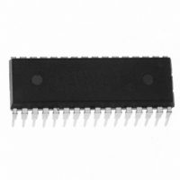
... Plastic Dual In-Line Package (PDIP) –A– –T– SEATING PLANE MC68HC908JL8/JK8 • MC68HC08JL8/JK8 • MC68HC908KL8 Data Sheet, Rev. 3.1 Freescale Semiconductor 0.25 (0.010 0.25 (0.010) ...
Page 196
... BSC 0.100 BSC H 1.65 2.16 0.065 0.085 J 0.20 0.38 0.008 0.015 K 2.92 3.43 0.115 0.135 L 15.24 BSC 0.600 BSC M 0° 15° 0° 15° N 0.51 1.02 0.020 0.040 Freescale Semiconductor MAX 0.510 0.299 0.104 0.019 0.035 0.012 0.009 7 0.415 0.029 ...
Page 197
... Shrink Dual In-Line Package (SDIP 10.46 9.86 1 4.35 1.778 30X 4.05 0.75 0.889 2X 0.45 2.49 2.39 MC68HC908JL8/JK8 • MC68HC08JL8/JK8 • MC68HC908KL8 Data Sheet, Rev. 3.1 Freescale Semiconductor 28-Pin Small Outline Integrated Circuit Package (SOIC 14X 0.010 (0.25 -T- ...
Page 198
... M 12 REF 12 REF N 0.090 0.160 0.004 0.006 P 0.400 BSC 0.016 BSC 0.150 0.250 0.006 0.010 S 9.000 BSC 0.354 BSC S1 4.500 BSC 0.177 BSC V 9.000 BSC 0.354 BSC V1 4.500 BSC 0.177 BSC W 0.200 REF 0.008 REF X 1.000 REF 0.039 REF Freescale Semiconductor ...
Page 199
... MC68HC908JL8MDW MC68HC908JL8CSP MC68HC908JL8MSP MC68HC908JL8CFA MC68HC908JL8MFA NOTE: Temperature grade "M" is available for V MC68HC908JL8/JK8 • MC68HC08JL8/JK8 • MC68HC908KL8 Data Sheet, Rev. 3.1 Freescale Semiconductor Table 19-1. MC Order Numbers Operating Temperature Range –40 °C to +85 °C –40 °C to +125 °C –40 °C to +85 °C – ...
Page 200
... Ordering Information MC68HC908JL8/JK8 • MC68HC08JL8/JK8 • MC68HC908KL8 Data Sheet, Rev. 3.1 200 Freescale Semiconductor ...