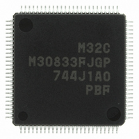
M30833FJGP#U3 Renesas Electronics America, M30833FJGP#U3 Datasheet - Page 517

M30833FJGP#U3
Manufacturer Part Number
M30833FJGP#U3
Description
IC M32C/83 MCU FLASH 100LQFP
Manufacturer
Renesas Electronics America
Series
M16C™ M32C/80r
Datasheets
1.M3087BFLGPU3.pdf
(364 pages)
2.M30833FJGPU3.pdf
(96 pages)
3.M30833FJGPU3.pdf
(529 pages)
Specifications of M30833FJGP#U3
Core Processor
M32C/80
Core Size
16/32-Bit
Speed
32MHz
Connectivity
CAN, I²C, IEBus, SIO, UART/USART
Peripherals
DMA, WDT
Number Of I /o
85
Program Memory Size
512KB (512K x 8)
Program Memory Type
FLASH
Ram Size
31K x 8
Voltage - Supply (vcc/vdd)
3 V ~ 5.5 V
Data Converters
A/D 26x10b; D/A 2x8b
Oscillator Type
Internal
Operating Temperature
-40°C ~ 85°C
Package / Case
100-LQFP
Package
100LQFP
Family Name
R8C
Maximum Speed
32 MHz
Operating Supply Voltage
5 V
Data Bus Width
16 Bit
Number Of Programmable I/os
87
Interface Type
UART
On-chip Adc
26-chx10-bit
On-chip Dac
2-chx8-bit
Number Of Timers
11
For Use With
R0K330879S001BE - KIT DEV RSK M32C/87R0K330879S000BE - KIT DEV RSK M32C/87
Lead Free Status / RoHS Status
Lead free / RoHS Compliant
Eeprom Size
-
Available stocks
Company
Part Number
Manufacturer
Quantity
Price
- Current page: 517 of 529
- Download datasheet (5Mb)
Rev.
1.10
REVISION HISTORY
2004-3
Date
All Pages Chapter numbers, section numbers, etc., added; Table and Figure numbers
15 to 18
24 to 45
Page
9, 13
2, 3
20
23
46
47
48
49
50
4
5
Overview
• Tables 1.1 and 1.2 M32C/83 Group Performance
• Figure 1.1 M32C/83 Block Diagram modified
• Table 1.3 M32C/83 Group Product deleted
• Tables 1.4 and 1.5 Pin Characteristics VREF pin changed from “analog pin”
• Table 1.6 Pin Description SDA0 to SDA4 changed from “output” to “input”;
Centeral Processing Unit
• Figure 2.1 CPU Register modified
Memory
• Figure 3.1 Memory Map Product deleted; Diagram modified
SFR
Value after reset and lisiting sequence modified
• “? : Indetermination” changed to “X : Indeterminate”
• Notation “Users cannot use any symbols with *” deleted
• Register names, symbols, and Values after RESET of addresses 001F
• Notations added to PM0 and TCSPR registers
• Value after reset in the RLVL register modified
Reset
• Figure 5.1 Reset Circuit modified
• Figure 5.2 Reset Sequence Diagram modified; Note 1 added
• 5.3 Watchdog Timer Reset added
• Figure 5.3 CPU Register after Reset modified
Processor Mode
• 6.2.2 Applying V
modified; Chapter sequence modified; Word Phrasing in Revision History
changed
Shortest Instruction Execution Time modified: 31.3ns(f(BCLK)=30MHz
changed to 31.3ns(f(BCLK)=32MHz, 50ns(f(BCLK)=20MHz added;
Performance details of Multifunction Timer, Intelligent I/O, Clock Generating
Circuit, and Electrical Characteristics revised;
Oscillator Stop Detect Function added;
32MHz added to Supply Voltage and Power Consumption
Note 3 added
to “control pin”
Descriptions of A/D-related pin functions revised
0025
deleted
16
, 0030
M32C/83 GROUP (M32C/83, M32C/83T) Hardware Manual
16
to 0035
CC
to CNV
C-4
16
, 0055
Description
SS
Pin Contents added
16
Summary
to 0056
16
, 01AC
16
, and 01AE
16
to 01BF
16
to
16
Related parts for M30833FJGP#U3
Image
Part Number
Description
Manufacturer
Datasheet
Request
R

Part Number:
Description:
KIT STARTER FOR M16C/29
Manufacturer:
Renesas Electronics America
Datasheet:

Part Number:
Description:
KIT STARTER FOR R8C/2D
Manufacturer:
Renesas Electronics America
Datasheet:

Part Number:
Description:
R0K33062P STARTER KIT
Manufacturer:
Renesas Electronics America
Datasheet:

Part Number:
Description:
KIT STARTER FOR R8C/23 E8A
Manufacturer:
Renesas Electronics America
Datasheet:

Part Number:
Description:
KIT STARTER FOR R8C/25
Manufacturer:
Renesas Electronics America
Datasheet:

Part Number:
Description:
KIT STARTER H8S2456 SHARPE DSPLY
Manufacturer:
Renesas Electronics America
Datasheet:

Part Number:
Description:
KIT STARTER FOR R8C38C
Manufacturer:
Renesas Electronics America
Datasheet:

Part Number:
Description:
KIT STARTER FOR R8C35C
Manufacturer:
Renesas Electronics America
Datasheet:

Part Number:
Description:
KIT STARTER FOR R8CL3AC+LCD APPS
Manufacturer:
Renesas Electronics America
Datasheet:

Part Number:
Description:
KIT STARTER FOR RX610
Manufacturer:
Renesas Electronics America
Datasheet:

Part Number:
Description:
KIT STARTER FOR R32C/118
Manufacturer:
Renesas Electronics America
Datasheet:

Part Number:
Description:
KIT DEV RSK-R8C/26-29
Manufacturer:
Renesas Electronics America
Datasheet:

Part Number:
Description:
KIT STARTER FOR SH7124
Manufacturer:
Renesas Electronics America
Datasheet:

Part Number:
Description:
KIT STARTER FOR H8SX/1622
Manufacturer:
Renesas Electronics America
Datasheet:

Part Number:
Description:
KIT DEV FOR SH7203
Manufacturer:
Renesas Electronics America
Datasheet:


