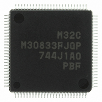
M30833FJGP#U3 Renesas Electronics America, M30833FJGP#U3 Datasheet - Page 103

M30833FJGP#U3
Manufacturer Part Number
M30833FJGP#U3
Description
IC M32C/83 MCU FLASH 100LQFP
Manufacturer
Renesas Electronics America
Series
M16C™ M32C/80r
Datasheets
1.M3087BFLGPU3.pdf
(364 pages)
2.M30833FJGPU3.pdf
(96 pages)
3.M30833FJGPU3.pdf
(529 pages)
Specifications of M30833FJGP#U3
Core Processor
M32C/80
Core Size
16/32-Bit
Speed
32MHz
Connectivity
CAN, I²C, IEBus, SIO, UART/USART
Peripherals
DMA, WDT
Number Of I /o
85
Program Memory Size
512KB (512K x 8)
Program Memory Type
FLASH
Ram Size
31K x 8
Voltage - Supply (vcc/vdd)
3 V ~ 5.5 V
Data Converters
A/D 26x10b; D/A 2x8b
Oscillator Type
Internal
Operating Temperature
-40°C ~ 85°C
Package / Case
100-LQFP
Package
100LQFP
Family Name
R8C
Maximum Speed
32 MHz
Operating Supply Voltage
5 V
Data Bus Width
16 Bit
Number Of Programmable I/os
87
Interface Type
UART
On-chip Adc
26-chx10-bit
On-chip Dac
2-chx8-bit
Number Of Timers
11
For Use With
R0K330879S001BE - KIT DEV RSK M32C/87R0K330879S000BE - KIT DEV RSK M32C/87
Lead Free Status / RoHS Status
Lead free / RoHS Compliant
Eeprom Size
-
Available stocks
Company
Part Number
Manufacturer
Quantity
Price
- Current page: 103 of 529
- Download datasheet (5Mb)
R
R
M
e
E
3
. v
J
Figure 8.12 External Circuit with PLL Frequency Synthesizer
Table 8.2 Bit Settings to Use PLL Clock as CPU Clock Source
Figure 8.13 Procedure to Use PLL Clock as CPU Clock Source
2
10MHz
8MHz
0
f(X
1
C
9
3 .
B
8 /
IN
0
1
3
0
)
3
J
G
4
a
0 -
o r
n
Microcomputer
3 .
1
u
3
, 1
C1=220pF, C2=0.1 µF, R1=1 k
p
V
1
PLC02
CONT
(
2
P8
V
M
0
0
1
SS
0
3
6
6
2
C
Use PLL clock as CPU clock source
8 /
Page 78
(PLL clock as CPU clock source)
, 3
PLC0 Register
(PLL clock division enabled)
Set the PLC02 to PLC00 bits
M
Set the PLC11 bit to "1"
Set the PLC07 bit to "1"
Set the CM17 bit to "1"
PLC01
C1
3
and the PLC12 bit
1
0
2
Wait 20 to 50ms
R1
C
f o
8 /
(PLL on)
4
3
End
8
) T
8
(2)
PLC00
C2
1
0
NOTES:
1. Connect V
2. Optimal values of the low pass filter circuit element,
wiring. Ground pattern must be formed around the circuit.
connected to the V
(e.g.noise). Evaluate not only with these optimal values, but
also with other values, to determine the values most
appropriate for your system.
Use capacitors for temperature compensation.
PLC1 Register
PLC12
SS
0
1
0
1
PLC11 and PLC12 bits : Bit in PLC1 register
PLC00 to PLC02 bits, PLC07 bit : Bits in PLC0 register
CM17 bit : Bit in CM1 register
to GND via C1 and C2 with shortest possible
CONT
PLL Clock
pin, varies with environment
30 MHz
20 MHz
21.3MHz
32MHz
8. Clock Generation Circuit
Related parts for M30833FJGP#U3
Image
Part Number
Description
Manufacturer
Datasheet
Request
R

Part Number:
Description:
KIT STARTER FOR M16C/29
Manufacturer:
Renesas Electronics America
Datasheet:

Part Number:
Description:
KIT STARTER FOR R8C/2D
Manufacturer:
Renesas Electronics America
Datasheet:

Part Number:
Description:
R0K33062P STARTER KIT
Manufacturer:
Renesas Electronics America
Datasheet:

Part Number:
Description:
KIT STARTER FOR R8C/23 E8A
Manufacturer:
Renesas Electronics America
Datasheet:

Part Number:
Description:
KIT STARTER FOR R8C/25
Manufacturer:
Renesas Electronics America
Datasheet:

Part Number:
Description:
KIT STARTER H8S2456 SHARPE DSPLY
Manufacturer:
Renesas Electronics America
Datasheet:

Part Number:
Description:
KIT STARTER FOR R8C38C
Manufacturer:
Renesas Electronics America
Datasheet:

Part Number:
Description:
KIT STARTER FOR R8C35C
Manufacturer:
Renesas Electronics America
Datasheet:

Part Number:
Description:
KIT STARTER FOR R8CL3AC+LCD APPS
Manufacturer:
Renesas Electronics America
Datasheet:

Part Number:
Description:
KIT STARTER FOR RX610
Manufacturer:
Renesas Electronics America
Datasheet:

Part Number:
Description:
KIT STARTER FOR R32C/118
Manufacturer:
Renesas Electronics America
Datasheet:

Part Number:
Description:
KIT DEV RSK-R8C/26-29
Manufacturer:
Renesas Electronics America
Datasheet:

Part Number:
Description:
KIT STARTER FOR SH7124
Manufacturer:
Renesas Electronics America
Datasheet:

Part Number:
Description:
KIT STARTER FOR H8SX/1622
Manufacturer:
Renesas Electronics America
Datasheet:

Part Number:
Description:
KIT DEV FOR SH7203
Manufacturer:
Renesas Electronics America
Datasheet:


