M30833FJGP#U3 Renesas Electronics America, M30833FJGP#U3 Datasheet - Page 341
M30833FJGP#U3
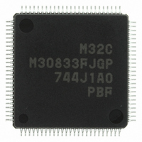
Manufacturer Part Number
M30833FJGP#U3
Description
IC M32C/83 MCU FLASH 100LQFP
Manufacturer
Renesas Electronics America
Series
M16C™ M32C/80r
Datasheets
1.M3087BFLGPU3.pdf
(364 pages)
2.M30833FJGPU3.pdf
(96 pages)
3.M30833FJGPU3.pdf
(529 pages)
Specifications of M30833FJGP#U3
Core Processor
M32C/80
Core Size
16/32-Bit
Speed
32MHz
Connectivity
CAN, I²C, IEBus, SIO, UART/USART
Peripherals
DMA, WDT
Number Of I /o
85
Program Memory Size
512KB (512K x 8)
Program Memory Type
FLASH
Ram Size
31K x 8
Voltage - Supply (vcc/vdd)
3 V ~ 5.5 V
Data Converters
A/D 26x10b; D/A 2x8b
Oscillator Type
Internal
Operating Temperature
-40°C ~ 85°C
Package / Case
100-LQFP
Package
100LQFP
Family Name
R8C
Maximum Speed
32 MHz
Operating Supply Voltage
5 V
Data Bus Width
16 Bit
Number Of Programmable I/os
87
Interface Type
UART
On-chip Adc
26-chx10-bit
On-chip Dac
2-chx8-bit
Number Of Timers
11
For Use With
R0K330879S001BE - KIT DEV RSK M32C/87R0K330879S000BE - KIT DEV RSK M32C/87
Lead Free Status / RoHS Status
Lead free / RoHS Compliant
Eeprom Size
-
Available stocks
Company
Part Number
Manufacturer
Quantity
Price


M
R
R
e
E
3
. v
J
2
NOTES:
NOTES:
´
NOTES:
Table 21.38 Pin Settings (1)
Table 21.39 Pin Settings (2)
Table 21.40 Pin Settings (3)
9 0
C
Name
Name
. 1
P13
P13
Name
Port
P9
P9
Port
P7
P7
1. P7
2. Set the MOD2 to MOD0 bits in the G2POCR0 register to "111
1. Set the MOD2 to MOD0 bits in the G2POCR0 register to "111
2. Set the PD9 and PS3 registers immediately after the PRC2 bit in the PRCR register is set to "1" (write
1. Set the MOD2 to MOD0 bits in the G2POCR0 register to "111
8 /
B
Port
1 3
0
1
2
3
0 (1)
1
enable). Do not generate an interrupt or a DMA transfer between the instruction to set to the PRC2 bit to "1"
and the instruction to set the PD9 and PS3 registers.
4
5
3 0
G
J
- 4
n a
0
o r
IE
IE
IE
IE
1 0
is a port for the N-channel open drain output.
3 .
u
IE
IE
IN
OUT
Function
OUT
IN
Function
p
, 1
1 3
Function
OUT
IN
input
input
(
0 2
M
output PS3_2 = 1
input
output
3
6 0
output PS1_0 = 1
2
C
8 /
Page 316
PS3 Register
PS3_1 = 0
, 3
PS7 Register PSL7 Register IPS Register
PS7_4 = 1
PS7_5 = 0
PS1 Register PSL1 Register PSC Register PD7 Register IPS Register
PS1_1 = 0
M
3
2
C
f o
8 /
4
3
(2)
8 8
) T
PSL3 Register PD9 Register
PSL3_2 = 1
-
PD13_5 = 0
-
Bit and Setting
PSL1_0 = 0
-
Bit and Setting
PD9_2 = 0
-
IPS5 to 4 = 10
-
Bit and Setting
PSC_0 = 1
-
21. Intelligent I/O (Group 2 Communication Function)
(2)
2
G2POCR0
-
-
PD7_1 = 0
IPS Register
IPS5 to 4 = 01
-
Register
2
2
2
".
".
".
(1)
2
-
G2POCR0
-
IPS5 to 4 = 00
Register
(1)
2
G2POCR0
-
Register
(2)
Related parts for M30833FJGP#U3
Image
Part Number
Description
Manufacturer
Datasheet
Request
R

Part Number:
Description:
KIT STARTER FOR M16C/29
Manufacturer:
Renesas Electronics America
Datasheet:

Part Number:
Description:
KIT STARTER FOR R8C/2D
Manufacturer:
Renesas Electronics America
Datasheet:

Part Number:
Description:
R0K33062P STARTER KIT
Manufacturer:
Renesas Electronics America
Datasheet:

Part Number:
Description:
KIT STARTER FOR R8C/23 E8A
Manufacturer:
Renesas Electronics America
Datasheet:

Part Number:
Description:
KIT STARTER FOR R8C/25
Manufacturer:
Renesas Electronics America
Datasheet:

Part Number:
Description:
KIT STARTER H8S2456 SHARPE DSPLY
Manufacturer:
Renesas Electronics America
Datasheet:

Part Number:
Description:
KIT STARTER FOR R8C38C
Manufacturer:
Renesas Electronics America
Datasheet:

Part Number:
Description:
KIT STARTER FOR R8C35C
Manufacturer:
Renesas Electronics America
Datasheet:

Part Number:
Description:
KIT STARTER FOR R8CL3AC+LCD APPS
Manufacturer:
Renesas Electronics America
Datasheet:
Part Number:
Description:
KIT STARTER FOR RX610
Manufacturer:
Renesas Electronics America
Datasheet:

Part Number:
Description:
KIT STARTER FOR R32C/118
Manufacturer:
Renesas Electronics America
Datasheet:

Part Number:
Description:
KIT DEV RSK-R8C/26-29
Manufacturer:
Renesas Electronics America
Datasheet:

Part Number:
Description:
KIT STARTER FOR SH7124
Manufacturer:
Renesas Electronics America
Datasheet:

Part Number:
Description:
KIT STARTER FOR H8SX/1622
Manufacturer:
Renesas Electronics America
Datasheet:

Part Number:
Description:
KIT DEV FOR SH7203
Manufacturer:
Renesas Electronics America
Datasheet: