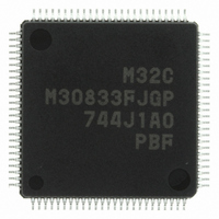
M30833FJGP#U3 Renesas Electronics America, M30833FJGP#U3 Datasheet - Page 416

M30833FJGP#U3
Manufacturer Part Number
M30833FJGP#U3
Description
IC M32C/83 MCU FLASH 100LQFP
Manufacturer
Renesas Electronics America
Series
M16C™ M32C/80r
Datasheets
1.M3087BFLGPU3.pdf
(364 pages)
2.M30833FJGPU3.pdf
(96 pages)
3.M30833FJGPU3.pdf
(529 pages)
Specifications of M30833FJGP#U3
Core Processor
M32C/80
Core Size
16/32-Bit
Speed
32MHz
Connectivity
CAN, I²C, IEBus, SIO, UART/USART
Peripherals
DMA, WDT
Number Of I /o
85
Program Memory Size
512KB (512K x 8)
Program Memory Type
FLASH
Ram Size
31K x 8
Voltage - Supply (vcc/vdd)
3 V ~ 5.5 V
Data Converters
A/D 26x10b; D/A 2x8b
Oscillator Type
Internal
Operating Temperature
-40°C ~ 85°C
Package / Case
100-LQFP
Package
100LQFP
Family Name
R8C
Maximum Speed
32 MHz
Operating Supply Voltage
5 V
Data Bus Width
16 Bit
Number Of Programmable I/os
87
Interface Type
UART
On-chip Adc
26-chx10-bit
On-chip Dac
2-chx8-bit
Number Of Timers
11
For Use With
R0K330879S001BE - KIT DEV RSK M32C/87R0K330879S000BE - KIT DEV RSK M32C/87
Lead Free Status / RoHS Status
Lead free / RoHS Compliant
Eeprom Size
-
Available stocks
Company
Part Number
Manufacturer
Quantity
Price
- Current page: 416 of 529
- Download datasheet (5Mb)
R
R
M
25.1 Memory Map
e
E
3
. v
J
Figure 25.1 Flash Memory Block Diagram
2
0
The flash memory contains a user ROM area, with space to store microcomputer operating programs in
single-chip mode or memory expansion mode, and a separate 8-Kbyte boot ROM area. Figure 25.1 shows
a block diagram of the flash memory.
The user ROM area is divided into several blocks, each of which can be protected (locked) from program
and erase. The user ROM area can be rewritten in CPU rewrite, standard serial I/O and parallel I/O modes.
The boot ROM area is allocated in the same addresses as the user ROM area. It can only be rewritten in
parallel I/O mode (refer to 25.5 Parallel I/O Mode). A program in the boot ROM area is executed after a
hardware reset occurs while an "H" signal is applied to the CNV
to the P5
reset occurs while an "L" signal is applied to the CNV
read.
1
9
C
3 .
B
8 /
0
1
3
0
3
J
F80000
F90000
FA0000
FB0000
FC0000
FD0000
FE0000
FF0000
G
FFA000
FFC000
FFFFFF
FF8000
4
a
0 -
n
o r
3 .
5
1
u
, 1
3
pin (refer to 25.1.1 Boot Mode). A program in the user ROM area is executed after a hardware
p
1
16
16
16
16
16
16
16
16
2
16
16
16
(
16
M
0
0
3
6
2
C
Page 391
8 /
Block 10 : 64 Kbytes
, 3
Block 9 : 64 Kbytes
Block 8 : 64 Kbytes
Block 7 : 64 Kbytes
Block 6 : 64 Kbytes
Block 5 : 64 Kbytes
Block 4 : 64 Kbytes
Block 1 : 8 Kbytes
Block 2 : 8 Kbytes
Block 0 : 16 Kbytes
User ROM Area
Block 3 : 32 Kbytes
M
3
2
C
f o
8 /
4
3
8
) T
8
NOTES:
FFE000
FFFFFF
SS
1. The boot ROM area can be rewritten in parallel I/O
mode
2. When specifying a block, use the highest-order even
only. (Refer to 25.5.1 Boot Mode)
address in the block to be specified.
16
16
pin. Consequently, the boot ROM area cannot be
SS
and P5
Boot ROM Area
8 Kbytes
0
pins and an "L" signal is applied
25. Flash Memory Version
Related parts for M30833FJGP#U3
Image
Part Number
Description
Manufacturer
Datasheet
Request
R

Part Number:
Description:
KIT STARTER FOR M16C/29
Manufacturer:
Renesas Electronics America
Datasheet:

Part Number:
Description:
KIT STARTER FOR R8C/2D
Manufacturer:
Renesas Electronics America
Datasheet:

Part Number:
Description:
R0K33062P STARTER KIT
Manufacturer:
Renesas Electronics America
Datasheet:

Part Number:
Description:
KIT STARTER FOR R8C/23 E8A
Manufacturer:
Renesas Electronics America
Datasheet:

Part Number:
Description:
KIT STARTER FOR R8C/25
Manufacturer:
Renesas Electronics America
Datasheet:

Part Number:
Description:
KIT STARTER H8S2456 SHARPE DSPLY
Manufacturer:
Renesas Electronics America
Datasheet:

Part Number:
Description:
KIT STARTER FOR R8C38C
Manufacturer:
Renesas Electronics America
Datasheet:

Part Number:
Description:
KIT STARTER FOR R8C35C
Manufacturer:
Renesas Electronics America
Datasheet:

Part Number:
Description:
KIT STARTER FOR R8CL3AC+LCD APPS
Manufacturer:
Renesas Electronics America
Datasheet:

Part Number:
Description:
KIT STARTER FOR RX610
Manufacturer:
Renesas Electronics America
Datasheet:

Part Number:
Description:
KIT STARTER FOR R32C/118
Manufacturer:
Renesas Electronics America
Datasheet:

Part Number:
Description:
KIT DEV RSK-R8C/26-29
Manufacturer:
Renesas Electronics America
Datasheet:

Part Number:
Description:
KIT STARTER FOR SH7124
Manufacturer:
Renesas Electronics America
Datasheet:

Part Number:
Description:
KIT STARTER FOR H8SX/1622
Manufacturer:
Renesas Electronics America
Datasheet:

Part Number:
Description:
KIT DEV FOR SH7203
Manufacturer:
Renesas Electronics America
Datasheet:


