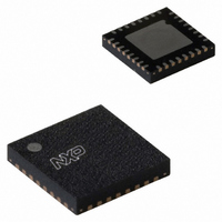
LPC1342FHN33,551 NXP Semiconductors, LPC1342FHN33,551 Datasheet - Page 32

LPC1342FHN33,551
Manufacturer Part Number
LPC1342FHN33,551
Description
IC MCU 32BIT 16KB FLASH 33HVQFN
Manufacturer
NXP Semiconductors
Series
LPC13xxr
Specifications of LPC1342FHN33,551
Program Memory Type
FLASH
Program Memory Size
16KB (16K x 8)
Package / Case
33-VQFN Exposed Pad, 33-HVQFN, 33-SQFN, 33-DHVQFN
Core Processor
ARM® Cortex-M3™
Core Size
32-Bit
Speed
72MHz
Connectivity
I²C, Microwire, SPI, SSI, SSP, UART/USART, USB
Peripherals
Brown-out Detect/Reset, POR, WDT
Number Of I /o
28
Ram Size
4K x 8
Voltage - Supply (vcc/vdd)
2 V ~ 3.6 V
Data Converters
A/D 8x10b
Oscillator Type
Internal
Operating Temperature
-40°C ~ 85°C
Processor Series
LPC13
Core
ARM Cortex M3
Data Bus Width
32 bit
Data Ram Size
4 KB
Interface Type
I2C, UART
Maximum Clock Frequency
72 MHz
Number Of Programmable I/os
28
Number Of Timers
4
Operating Supply Voltage
3.3 V
Maximum Operating Temperature
+ 85 C
Mounting Style
SMD/SMT
3rd Party Development Tools
MDK-ARM, RL-ARM, ULINK2
Minimum Operating Temperature
- 40 C
On-chip Adc
10 bit, 8 Channel
Package
33HVQFN EP
Device Core
ARM Cortex M3
Family Name
LPC1000
Maximum Speed
72 MHz
Lead Free Status / RoHS Status
Lead free / RoHS Compliant
For Use With
622-1005 - USB IN-CIRCUIT PROG ARM7 LPC2K
Eeprom Size
-
Lead Free Status / Rohs Status
Lead free / RoHS Compliant
Other names
568-4946
935289656551
935289656551
- Current page: 32 of 331
- Download datasheet (2Mb)
NXP Semiconductors
UM10375
User manual
3.5.37 Start logic signal enable register 0
Table 41.
This STARTERP0 register enables or disables the start signal bits in the start logic. The bit
assignment is identical to
Table 42.
Bit
11:1
12
23:13 APRPIO1_11
24
31:25 APRPIO2_7
Bit
0
11:1
12
23:13 ERPIO1_11 to
24
Symbol
ERPIO0_0
ERPIO0_11 to
ERPIO_0_1
ERPIO1_0
ERPIO1_1
ERPIO2_0
Symbol
APRPIO0_11
to
APRPIO0_1
APRPIO1_0
to
APRPIO1_1
APRPIO2_0
to
APRPIO2_1
Start logic edge control register 0 (STARTAPRP0, address 0x4004 8200) bit
description
Start logic signal enable register 0 (STARTERP0, address 0x4004 8204) bit
description
All information provided in this document is subject to legal disclaimers.
Value
0
1
0
1
0
1
0
1
0
1
Value
0
1
0
1
0
1
0
1
0
1
…continued
Rev. 2 — 7 July 2010
Table
Description
Enable start signal for start logic input PIO0_0
Disabled
Enabled
Enable start signal for start logic input PIO0_11 to
PIO0_1
Disabled
Enabled
Enable start signal for start logic input PIO1_0
Disabled
Enabled
Enable start signal for start logic input PIO1_11 to
PIO1_1
Disabled
Enabled
Enable start signal for start logic input PIO2_0
Disabled
Enabled
Description
Edge select for start logic input PIO0_11 to PIO0_1
Falling edge
Rising edge
Edge select for start logic input PIO1_0
Falling edge
Rising edge
Edge select for start logic input PIO1_11 to PIO1_1
Falling edge
Rising edge
Edge select for start logic input PIO2_0
Falling edge
Rising edge
Edge select for start logic input PIO2_7 to PIO2_1
Falling edge
Rising edge
41.
Chapter 3: LPC13xx System configuration
UM10375
© NXP B.V. 2010. All rights reserved.
Reset
value
0
0
0
0
0
Reset
value
0
0
0
0
0
33 of 333
Related parts for LPC1342FHN33,551
Image
Part Number
Description
Manufacturer
Datasheet
Request
R
Part Number:
Description:
NXP Semiconductors designed the LPC2420/2460 microcontroller around a 16-bit/32-bitARM7TDMI-S CPU core with real-time debug interfaces that include both JTAG andembedded trace
Manufacturer:
NXP Semiconductors
Datasheet:

Part Number:
Description:
NXP Semiconductors designed the LPC2458 microcontroller around a 16-bit/32-bitARM7TDMI-S CPU core with real-time debug interfaces that include both JTAG andembedded trace
Manufacturer:
NXP Semiconductors
Datasheet:
Part Number:
Description:
NXP Semiconductors designed the LPC2468 microcontroller around a 16-bit/32-bitARM7TDMI-S CPU core with real-time debug interfaces that include both JTAG andembedded trace
Manufacturer:
NXP Semiconductors
Datasheet:
Part Number:
Description:
NXP Semiconductors designed the LPC2470 microcontroller, powered by theARM7TDMI-S core, to be a highly integrated microcontroller for a wide range ofapplications that require advanced communications and high quality graphic displays
Manufacturer:
NXP Semiconductors
Datasheet:
Part Number:
Description:
NXP Semiconductors designed the LPC2478 microcontroller, powered by theARM7TDMI-S core, to be a highly integrated microcontroller for a wide range ofapplications that require advanced communications and high quality graphic displays
Manufacturer:
NXP Semiconductors
Datasheet:
Part Number:
Description:
The Philips Semiconductors XA (eXtended Architecture) family of 16-bit single-chip microcontrollers is powerful enough to easily handle the requirements of high performance embedded applications, yet inexpensive enough to compete in the market for hi
Manufacturer:
NXP Semiconductors
Datasheet:
Part Number:
Description:
The XA-S3 device is a member of Philips Semiconductors? XA(eXtended Architecture) family of high performance 16-bitsingle-chip microcontrollers
Manufacturer:
NXP Semiconductors
Datasheet:

Part Number:
Description:
The NXP BlueStreak LH75401/LH75411 family consists of two low-cost 16/32-bit System-on-Chip (SoC) devices
Manufacturer:
NXP Semiconductors
Datasheet:

Part Number:
Description:
The NXP LPC3130/3131 combine an 180 MHz ARM926EJ-S CPU core, high-speed USB2
Manufacturer:
NXP Semiconductors
Datasheet:

Part Number:
Description:
The NXP LPC3141 combine a 270 MHz ARM926EJ-S CPU core, High-speed USB 2
Manufacturer:
NXP Semiconductors

Part Number:
Description:
The NXP LPC3143 combine a 270 MHz ARM926EJ-S CPU core, High-speed USB 2
Manufacturer:
NXP Semiconductors

Part Number:
Description:
The NXP LPC3152 combines an 180 MHz ARM926EJ-S CPU core, High-speed USB 2
Manufacturer:
NXP Semiconductors

Part Number:
Description:
The NXP LPC3154 combines an 180 MHz ARM926EJ-S CPU core, High-speed USB 2
Manufacturer:
NXP Semiconductors

Part Number:
Description:
Standard level N-channel enhancement mode Field-Effect Transistor (FET) in a plastic package using NXP High-Performance Automotive (HPA) TrenchMOS technology
Manufacturer:
NXP Semiconductors
Datasheet:


