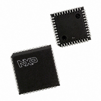
P89V52X2FA,512 NXP Semiconductors, P89V52X2FA,512 Datasheet - Page 37

P89V52X2FA,512
Manufacturer Part Number
P89V52X2FA,512
Description
IC 80C51 MCU FLASH 8K 44-PLCC
Manufacturer
NXP Semiconductors
Series
89Vr
Datasheet
1.P89V52X2FA512.pdf
(57 pages)
Specifications of P89V52X2FA,512
Program Memory Type
FLASH
Program Memory Size
8KB (8K x 8)
Package / Case
44-PLCC
Core Processor
8051
Core Size
8-Bit
Speed
40MHz
Connectivity
UART/USART
Peripherals
POR
Number Of I /o
32
Eeprom Size
192 x 8
Ram Size
256 x 8
Voltage - Supply (vcc/vdd)
2.7 V ~ 5.5 V
Oscillator Type
External
Operating Temperature
-40°C ~ 85°C
Processor Series
P89V5x
Core
80C51
Data Bus Width
8 bit
Data Ram Size
256 B
Interface Type
UART
Maximum Clock Frequency
40 MHz
Number Of Programmable I/os
32
Number Of Timers
3
Operating Supply Voltage
2.7 V to 5.5 V
Maximum Operating Temperature
+ 125 C
Mounting Style
SMD/SMT
3rd Party Development Tools
PK51, CA51, A51, ULINK2
Minimum Operating Temperature
- 55 C
Lead Free Status / RoHS Status
Lead free / RoHS Compliant
For Use With
OM11011 - BOARD FOR P89V52X2 44-TQFP622-1017 - BOARD 44-ZIF PLCC SOCKET622-1012 - BOARD FOR P89V52X2 44-TQFP622-1008 - BOARD FOR LPC9103 10-HVSON622-1002 - USB IN-CIRCUIT PROG LPC9XX
Data Converters
-
Lead Free Status / Rohs Status
Lead free / RoHS Compliant
Other names
568-4249-5
935282528512
P89V52X2FA
935282528512
P89V52X2FA
Available stocks
Company
Part Number
Manufacturer
Quantity
Price
Company:
Part Number:
P89V52X2FA,512
Manufacturer:
NXP Semiconductors
Quantity:
10 000
NXP Semiconductors
Table 34.
P89V52X2_3
Product data sheet
Bit
0
1
2
3
4
5
6
7
Symbol
ERR
FMCMD.0
SV
FMCMD.1
-
FMCMD.2
-
FMCMD.3
DAP
FMCMD.4
-
FMCMD.5
WE
FMCMD.6
BUSY
FMCMD.7
Flash Memory Control register (FMCON - address E4H) bit description
Access
R
W
R
W
R
W
R
W
R
W
R
W
R
W
R
W
An assembly language routine to load the page register and perform an erase/program
operation is shown below. This code assumes the data EEPROM has been mapped into
user code space.
Description
Set when either of the following conditions occur:
Command byte bit 0.
Security violation. Set when an attempt is made to program, erase, or CRC a secured page.
The specific cause of the security violation depends on the operation:
Command byte bit 1
Reserved
Command byte bit 2.
Reserved
Command byte bit 3.
Data Access Protect. When set, access to the data EEPROM is unmapped and thus
prohibited. Set by the MAP command. Cleared by the UNMAP command.
Command byte bit 4.
Reserved
Command byte bit 5.
When set, indicates that data EEPROM writes during program execution are enabled.
Command byte bit 6.
Indicates that a program, erase, CRC calculation or similar operation is in progress. Note that
this bit is usable only in ICP mode since the CPU is stalled whenever this bit is set in execution
mode.
Command byte bit 7.
;**************************************************
;*
;**************************************************
;*
;* Inputs:
;*R3 = number of bytes to program (byte)
;*R4 = page address MSB(byte)
;*R5 = page address LSB(byte)
;*R7 = pointer to data buffer in RAM(byte)
;* Outputs:
;*R7 = status (byte)
;* C = clear on no error, set on error
;**************************************************
•
•
•
•
•
•
•
Device was reset before the operation was completed.
Attempt made to access data EEPROM while Data Access Protect (DAP) is set.
An error occurs in the device’s internal high voltage circuits.
PROG or EP: CSEC.0 = 1 or DPxSEC.1 = 1 for the page addressed by FMADRH/L.
ERS_G: Any DPxSEC.0 = 1.
ERS_DP: DPxSEC.2 = 1 for addressed page while in execution mode.
CRC_DP: DPxCSEC.0 = 1 and DPxSEC.1 = 0.
pgm user code
Rev. 03 — 4 May 2009
*
80C51 with 256 B RAM, 192 B data EEPROM
*
*
*
*
*
*
*
P89V52X2
© NXP B.V. 2009. All rights reserved.
*
*
37 of 57


