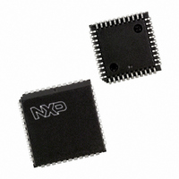
P89V52X2FA,512 NXP Semiconductors, P89V52X2FA,512 Datasheet - Page 14

P89V52X2FA,512
Manufacturer Part Number
P89V52X2FA,512
Description
IC 80C51 MCU FLASH 8K 44-PLCC
Manufacturer
NXP Semiconductors
Series
89Vr
Datasheet
1.P89V52X2FA512.pdf
(57 pages)
Specifications of P89V52X2FA,512
Program Memory Type
FLASH
Program Memory Size
8KB (8K x 8)
Package / Case
44-PLCC
Core Processor
8051
Core Size
8-Bit
Speed
40MHz
Connectivity
UART/USART
Peripherals
POR
Number Of I /o
32
Eeprom Size
192 x 8
Ram Size
256 x 8
Voltage - Supply (vcc/vdd)
2.7 V ~ 5.5 V
Oscillator Type
External
Operating Temperature
-40°C ~ 85°C
Processor Series
P89V5x
Core
80C51
Data Bus Width
8 bit
Data Ram Size
256 B
Interface Type
UART
Maximum Clock Frequency
40 MHz
Number Of Programmable I/os
32
Number Of Timers
3
Operating Supply Voltage
2.7 V to 5.5 V
Maximum Operating Temperature
+ 125 C
Mounting Style
SMD/SMT
3rd Party Development Tools
PK51, CA51, A51, ULINK2
Minimum Operating Temperature
- 55 C
Lead Free Status / RoHS Status
Lead free / RoHS Compliant
For Use With
OM11011 - BOARD FOR P89V52X2 44-TQFP622-1017 - BOARD 44-ZIF PLCC SOCKET622-1012 - BOARD FOR P89V52X2 44-TQFP622-1008 - BOARD FOR LPC9103 10-HVSON622-1002 - USB IN-CIRCUIT PROG LPC9XX
Data Converters
-
Lead Free Status / Rohs Status
Lead free / RoHS Compliant
Other names
568-4249-5
935282528512
P89V52X2FA
935282528512
P89V52X2FA
Available stocks
Company
Part Number
Manufacturer
Quantity
Price
Company:
Part Number:
P89V52X2FA,512
Manufacturer:
NXP Semiconductors
Quantity:
10 000
NXP Semiconductors
P89V52X2_3
Product data sheet
6.6 Reset
Table 9.
At initial power-up, the port pins will be in a random state until the oscillator has started
and the internal reset algorithm has weakly pulled all pins HIGH. Powering up the device
without a valid reset could cause the device to start executing instructions from an
indeterminate location. Such undefined states may inadvertently corrupt the code in the
flash. A system reset will not affect the on-chip RAM while the device is running, however,
the contents of the on-chip RAM during power-up are indeterminate.
When power is applied to the device, the RST pin must be held HIGH long enough for the
oscillator to start-up (usually several milliseconds for a low frequency crystal), in addition
to two machine cycles for a valid power-on reset. An example of a method to extend the
RST signal is to implement a RC circuit by connecting the RST pin to V
capacitor and to V
During initial power the POF flag in the PCON register is set to indicate an initial power-up
condition. The POF flag will remain active until cleared by software.
Following a reset condition, under normal conditions, the device will start executing code
from address 0000H in the user’s code memory. However if the requirements are met for
ICP entry, the device will enter ICP mode.
Bit
7 to 4
3
2
1
0
Fig 9. Power-on reset circuit
AUXR1 - Auxiliary register 1 (address A2H) bit description
Symbol
-
GF2
0
-
DPS
SS
through an 8.2 k resistor as shown in
V
DD
Rev. 03 — 4 May 2009
Description
Reserved for future use. Should be set to ‘0’ by user programs.
General purpose user-defined flag.
This bit contains a hard-wired ‘0’. Allows toggling of the DPS bit by
incrementing AUXR1, without interfering with other bits in the register.
Reserved for future use. Should be set to ‘0’ by user programs.
Data pointer select. Chooses one of two Data Pointers for use by the
program. See text for details.
10 F
8.2 k
C 2
C 1
80C51 with 256 B RAM, 192 B data EEPROM
RST
XTAL2
XTAL1
V
002aaa543
Figure
DD
9.
P89V52X2
DD
© NXP B.V. 2009. All rights reserved.
through a 10 F
14 of 57


