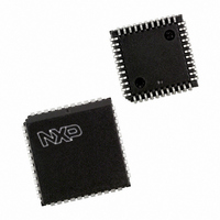
P89V52X2FA,512 NXP Semiconductors, P89V52X2FA,512 Datasheet - Page 32

P89V52X2FA,512
Manufacturer Part Number
P89V52X2FA,512
Description
IC 80C51 MCU FLASH 8K 44-PLCC
Manufacturer
NXP Semiconductors
Series
89Vr
Datasheet
1.P89V52X2FA512.pdf
(57 pages)
Specifications of P89V52X2FA,512
Program Memory Type
FLASH
Program Memory Size
8KB (8K x 8)
Package / Case
44-PLCC
Core Processor
8051
Core Size
8-Bit
Speed
40MHz
Connectivity
UART/USART
Peripherals
POR
Number Of I /o
32
Eeprom Size
192 x 8
Ram Size
256 x 8
Voltage - Supply (vcc/vdd)
2.7 V ~ 5.5 V
Oscillator Type
External
Operating Temperature
-40°C ~ 85°C
Processor Series
P89V5x
Core
80C51
Data Bus Width
8 bit
Data Ram Size
256 B
Interface Type
UART
Maximum Clock Frequency
40 MHz
Number Of Programmable I/os
32
Number Of Timers
3
Operating Supply Voltage
2.7 V to 5.5 V
Maximum Operating Temperature
+ 125 C
Mounting Style
SMD/SMT
3rd Party Development Tools
PK51, CA51, A51, ULINK2
Minimum Operating Temperature
- 55 C
Lead Free Status / RoHS Status
Lead free / RoHS Compliant
For Use With
OM11011 - BOARD FOR P89V52X2 44-TQFP622-1017 - BOARD 44-ZIF PLCC SOCKET622-1012 - BOARD FOR P89V52X2 44-TQFP622-1008 - BOARD FOR LPC9103 10-HVSON622-1002 - USB IN-CIRCUIT PROG LPC9XX
Data Converters
-
Lead Free Status / Rohs Status
Lead free / RoHS Compliant
Other names
568-4249-5
935282528512
P89V52X2FA
935282528512
P89V52X2FA
Available stocks
Company
Part Number
Manufacturer
Quantity
Price
Company:
Part Number:
P89V52X2FA,512
Manufacturer:
NXP Semiconductors
Quantity:
10 000
NXP Semiconductors
P89V52X2_3
Product data sheet
6.12.1 Idle mode
6.12 Power-saving modes
Table 26.
Table 27.
Bit addressable; Reset value: 00H
Table 28.
Table 29.
Not bit addressable; Reset value: 00H
Table 30.
The device provides two power saving modes of operation for applications where power
consumption is critical. The two modes are idle and Power-down, see
Idle mode is entered setting the IDL bit in the PCON register. In Idle mode, the program
counter is stopped. The system clock continues to run and all interrupts and peripherals
remain active. The on-chip RAM and the special function registers hold their data during
this mode.
Bit
2
1
0
Bit
7:6
5
4
3
2
1
0
Bit
7:6
5
4
3
2
1
0
Bit
Symbol
Bit
Symbol
IE - Interrupt enable register (address A8H) bit description
IP - Interrupt priority low register (address B8H) bit allocation
IP - Interrupt priority low register (address B8H) bit description
IPH - Interrupt priority high register (address B7H) bit allocation
IPH - Interrupt priority high register (address B7H) bit description
Symbol
EX1
ET0
EX0
Symbol
-
PT2
PS
PT1
PX1
PT0
PX0
Symbol
-
PT2H
PSH
PT1H
PX1H
PT0H
PX0H
7
7
-
-
6
6
-
-
Rev. 03 — 4 May 2009
Description
External Interrupt 1 Enable.
Timer 0 Overflow Interrupt Enable.
External Interrupt 0 Enable.
Description
Reserved
Timer 2 Interrupt Priority Low Bit.
Serial Port Interrupt Priority Low Bit.
Timer 1 Interrupt Priority Low Bit.
External Interrupt 1 Priority Low Bit.
Timer 0 Interrupt Priority Low Bit.
External Interrupt 0 Priority Low Bit.
Description
Reserved
Timer 2 Interrupt Priority High Bit.
Serial Port Interrupt Priority High Bit.
Timer 1 Interrupt Priority High Bit.
External Interrupt 1 Priority High Bit.
Timer 0 Interrupt Priority High Bit.
External Interrupt 0 Priority High Bit.
PT2H
PT2
5
5
PSH
80C51 with 256 B RAM, 192 B data EEPROM
PS
4
4
PT1H
PT1
3
3
PX1H
PX1
2
2
…continued
P89V52X2
Table
© NXP B.V. 2009. All rights reserved.
PT0H
PT0
1
1
31.
PX0H
PX0
32 of 57
0
0


