AT89C51ID2-RLTUM Atmel, AT89C51ID2-RLTUM Datasheet - Page 11
AT89C51ID2-RLTUM
Manufacturer Part Number
AT89C51ID2-RLTUM
Description
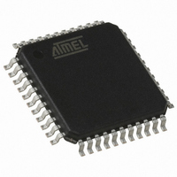
IC 8051 MCU FLASH 64K 44VQFP
Manufacturer
Atmel
Series
89Cr
Datasheet
1.AT89C51ID2-RLTUM.pdf
(157 pages)
Specifications of AT89C51ID2-RLTUM
Core Processor
8051
Core Size
8-Bit
Speed
60MHz
Connectivity
I²C, SPI, UART/USART
Peripherals
POR, PWM, WDT
Number Of I /o
34
Program Memory Size
64KB (64K x 8)
Program Memory Type
FLASH
Eeprom Size
2K x 8
Ram Size
2K x 8
Voltage - Supply (vcc/vdd)
2.7 V ~ 5.5 V
Oscillator Type
External
Operating Temperature
-40°C ~ 85°C
Package / Case
44-TQFP, 44-VQFP
Processor Series
AT89x
Core
8051
Data Bus Width
8 bit
Data Ram Size
2 KB
Interface Type
UART, SPI, TWI
Maximum Clock Frequency
60 MHz
Number Of Programmable I/os
34
Number Of Timers
3
Operating Supply Voltage
2.7 V to 5.5 V
Maximum Operating Temperature
+ 85 C
Mounting Style
SMD/SMT
3rd Party Development Tools
PK51, CA51, A51, ULINK2
Minimum Operating Temperature
- 40 C
Package
44VQFP
Device Core
8051
Family Name
89C
Maximum Speed
40 MHz
Height
1.45 mm
Length
10.1 mm
Supply Voltage (max)
5.5 V
Supply Voltage (min)
2.7 V
Width
10.1 mm
For Use With
AT89OCD-01 - USB EMULATOR FOR AT8XC51 MCU
Lead Free Status / RoHS Status
Lead free / RoHS Compliant
Data Converters
-
Lead Free Status / Rohs Status
Details
Available stocks
Company
Part Number
Manufacturer
Quantity
Price
Company:

Part Number:
AT89C51ID2-RLTUM
Manufacturer:
ATMEL
Quantity:
13 937


Table 15. Pin Description
11
V
V
P0.0 - P0.7
P1.0 - P1.7
SS
CC
Mnemonic
AT89C51ID2
PLCC44
43 - 36
2 - 9
22
44
2
3
4
5
6
7
8
9
Pin Number
VQFP44
37 - 30
40 - 44
1 - 3
16
38
40
41
42
43
44
1
2
3
Type
I/O
I/O
I/O
I/O
I/O
I/O
I/O
I/O
I/O
I/O
I/O
I/O
I/O
I/O
I/O
I/O
I/O
I/O
I
I
I
I
I
I
Name and Function
Ground: 0V reference
Power Supply: This is the power supply voltage for normal, idle and power-down opera-
tion
Port 0: Port 0 is an open-drain, bidirectional I/O port. Port 0 pins that have 1s written to
them float and can be used as high impedance inputs. Port 0 must be polarized to V
V
low-order address and data bus during access to external program and data memory. In
this application, it uses strong internal pull-up when emitting 1s. Port 0 also inputs the code
bytes during EPROM programming. External pull-ups are required during program verifica-
tion during which P0 outputs the code bytes.
Port 1: Port 1 is an 8-bit bidirectional I/O port with internal pull-ups. Port 1 pins that have 1s
written to them are pulled high by the internal pull-ups and can be used as inputs. As
inputs, Port 1 pins that are externally pulled low will source current because of the internal
pull-ups. Port 1 also receives the low-order address byte during memory programming and
verification.
Alternate functions for AT89C51ID2 Port 1 include:
P1.0: Input/Output
T2 (P1.0): Timer/Counter 2 external count input/Clockout
XTALB1 (P1.0): Sub Clock input to the inverting oscillator amplifier
P1.1: Input/Output
T2EX: Timer/Counter 2 Reload/Capture/Direction Control
SS: SPI Slave Select
P1.2: Input/Output
ECI: External Clock for the PCA
P1.3: Input/Output
CEX0: Capture/Compare External I/O for PCA module 0
P1.4: Input/Output
CEX1: Capture/Compare External I/O for PCA module 1
P1.5: Input/Output
CEX2: Capture/Compare External I/O for PCA module 2
MISO: SPI Master Input Slave Output line
When SPI is in master mode, MISO receives data from the slave peripheral. When SPI is in
slave mode, MISO outputs data to the master controller.
P1.6: Input/Output
CEX3: Capture/Compare External I/O for PCA module 3
SCK: SPI Serial Clock
P1.7: Input/Output:
CEX4: Capture/Compare External I/O for PCA module 4
SS
in order to prevent any parasitic current consumption. Port 0 is also the multiplexed
4289C–8051–11/05
CC
or
Related parts for AT89C51ID2-RLTUM
Image
Part Number
Description
Manufacturer
Datasheet
Request
R

Part Number:
Description:
Manufacturer:
Atmel Corporation
Datasheet:

Part Number:
Description:
IC 8051 MCU 64K FLASH 44-VQFP
Manufacturer:
Atmel
Datasheet:

Part Number:
Description:
IC 8051 MCU 64K FLASH 44-PLCC
Manufacturer:
Atmel
Datasheet:

Part Number:
Description:
8-bit Flash Microcontroller
Manufacturer:
ATMEL [ATMEL Corporation]
Datasheet:
Part Number:
Description:
8-bit Flash Microcontroller
Manufacturer:
ATMEL [ATMEL Corporation]
Datasheet:
Part Number:
Description:
IC 8051 MCU FLASH 64K 44PLCC
Manufacturer:
Atmel
Datasheet:
Part Number:
Description:
IC MCU FLASH 8051 64K 5V 44-PLCC
Manufacturer:
Atmel
Datasheet:
Part Number:
Description:
IC MCU FLASH 8051 64K 5V 44-VQFP
Manufacturer:
Atmel
Datasheet:
Part Number:
Description:
IC 8051 MCU FLASH 64K 44VQFP
Manufacturer:
Atmel
Datasheet:

Part Number:
Description:
C51ID2 64KF TWI 32KHZ PLCC44 3-5.5V IND.
Manufacturer:
Atmel
Datasheet:

Part Number:
Description:
IC MICRO CTRL 24MHZ 44TQFP
Manufacturer:
Atmel
Datasheet:
Part Number:
Description:
IC MICRO CTRL 24MHZ 44PLCC
Manufacturer:
Atmel
Datasheet:
Part Number:
Description:
IC MICRO CTRL 24MHZ 44PLCC
Manufacturer:
Atmel
Datasheet:

Part Number:
Description:
IC MICRO CTRL 24MHZ 40DIP
Manufacturer:
Atmel
Datasheet:
Part Number:
Description:
IC MICRO CTRL 24MHZ 40DIP
Manufacturer:
Atmel
Datasheet: