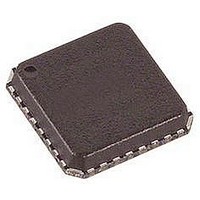
ADAU1381BCPZ Analog Devices Inc, ADAU1381BCPZ Datasheet - Page 44

ADAU1381BCPZ
Manufacturer Part Number
ADAU1381BCPZ
Description
IC AUDIO CODEC STEREO LN 32LFCSP
Manufacturer
Analog Devices Inc
Type
Stereo Audior
Datasheet
1.ADAU1381BCBZ-RL.pdf
(84 pages)
Specifications of ADAU1381BCPZ
Data Interface
Serial, SPI™
Resolution (bits)
24 b
Number Of Adcs / Dacs
2 / 2
Sigma Delta
No
S/n Ratio, Adcs / Dacs (db) Typ
97 / 100
Dynamic Range, Adcs / Dacs (db) Typ
96.5 / 100
Voltage - Supply, Analog
1.8 V ~ 3.65 V
Voltage - Supply, Digital
1.63 V ~ 3.65 V
Operating Temperature
-25°C ~ 85°C
Mounting Type
Surface Mount
Package / Case
32-VFQFN, CSP Exposed Pad
Audio Codec Type
Stereo
No. Of Adcs
2
No. Of Dacs
2
No. Of Input Channels
3
No. Of Output Channels
3
Adc / Dac Resolution
24bit
Adcs / Dacs Signal To Noise Ratio
100dB
Lead Free Status / RoHS Status
Lead free / RoHS Compliant
ADAU1381
CLOCK MANAGEMENT, INTERNAL REGULATOR,
AND PLL CONTROL
Register 16384 (0x4000), Clock Control
The clock control register sets the clocking scheme for the
ADAU1381. The system clock can be generated from either the
PLL or directly from the MCKI (master clock input) pin. Addi-
tionally, the MCKO (master clock output) pin can be configured.
Bits[6:5], MCKO Frequency
These bits set the frequency to be output on MCKO as a multiple
of the base sampling frequency (32×, 64×, 128×, or 256×). The
MCKO pin can be used to provide digital microphones with a clock.
Bit 4, MCKO Enable
This bit enables or disables the MCKO pin.
Bit 3, Clock Source Select
The clock source select bit either routes the MCLK input through
the PLL or bypasses the PLL. When using the PLL, the output of
Table 28. Clock Control Register
Bits
7
[6:5]
4
3
[2:1]
0
Table 29. Core Clock Output for f
MCLK Input Setting
256 × f
512 × f
768 × f
1024 × f
Table 30. Core Clock Output for f
MCLK Input Setting
256 × f
512 × f
768 × f
1024 × f
S
S
S
S
S
S
S
S
S
S
= 44.1 kHz
= 48 kHz
Description
Reserved
MCKO frequency
00: 32 × f
01: 64 × f
10: 128 × f
11: 256 × f
MCKO enable
0: disabled
1: enabled
Clock source select
0: direct from MCKI pin
1: PLL clock
Input master clock frequency
00: 256 × f
01: 512 × f
10: 768 × f
11: 1024 × f
Core clock enable
0: core clock disabled
1: core clock enabled
MCLK Input Value
11.2896 MHz
22.5792 MHz
33.8688 MHz
45.1584 MHz
MCLK Input Value
12.288 MHz
24.576 MHz
36.864 MHz
49.152 MHz
S
S
S
S
S
S
S
S
Rev. B | Page 44 of 84
MCLK Input Divider
1
2
3
4
MCLK Input Divider
1
2
3
4
the PLL is always 1024 × f
PLL parameters can be set in the PLL control register. Inputs
directly from MCKI require an exact clock rate as described in
the Bits[2:1], Input Master Clock Frequency section.
Bits[2:1], Input Master Clock Frequency
The maximum clock speed allowed is 1024 × 48 kHz. These bits set
the expected input master clock frequency for proper clock divider
values in order to output a constant system clock of 256 × f
using the PLL, these bits must always be set to 1024 × f
bypassing the PLL, the external clock frequency on the MCKI pin
must be 256 × f
Table 30 show the relationship between the system clock and the
internal master clock for base sampling frequencies of 44.1 kHz
and 48 kHz.
Bit 0, Core Clock Enable
This bit enables the internal master clock to start the IC.
S
, 512 × f
S
, 768 × f
S
, and Bits[2:1] should be set to 11.
S
, or 1024 × f
Default
00
0
0
00
0
Core Clock
11.2896 MHz
11.2896 MHz
11.2896 MHz
11.2896 MHz
Core Clock
12.288 MHz
12.288 MHz
12.288 MHz
12.288 MHz
S
. Table 29 and
S
. When
S
. When


