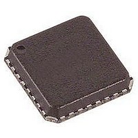
ADAU1381BCPZ Analog Devices Inc, ADAU1381BCPZ Datasheet - Page 36

ADAU1381BCPZ
Manufacturer Part Number
ADAU1381BCPZ
Description
IC AUDIO CODEC STEREO LN 32LFCSP
Manufacturer
Analog Devices Inc
Type
Stereo Audior
Datasheet
1.ADAU1381BCBZ-RL.pdf
(84 pages)
Specifications of ADAU1381BCPZ
Data Interface
Serial, SPI™
Resolution (bits)
24 b
Number Of Adcs / Dacs
2 / 2
Sigma Delta
No
S/n Ratio, Adcs / Dacs (db) Typ
97 / 100
Dynamic Range, Adcs / Dacs (db) Typ
96.5 / 100
Voltage - Supply, Analog
1.8 V ~ 3.65 V
Voltage - Supply, Digital
1.63 V ~ 3.65 V
Operating Temperature
-25°C ~ 85°C
Mounting Type
Surface Mount
Package / Case
32-VFQFN, CSP Exposed Pad
Audio Codec Type
Stereo
No. Of Adcs
2
No. Of Dacs
2
No. Of Input Channels
3
No. Of Output Channels
3
Adc / Dac Resolution
24bit
Adcs / Dacs Signal To Noise Ratio
100dB
Lead Free Status / RoHS Status
Lead free / RoHS Compliant
ADAU1381
SPI PORT
By default, the ADAU1381 is in I
control mode by pulling CLATCH low three times. The SPI port
uses a 4-wire interface, consisting of CLATCH , CCLK, CDATA,
and COUT signals, and is always a slave port. The CLATCH signal
goes low at the beginning of a transaction and high at the end of
a transaction. The CCLK signal latches CDATA on a low-to-high
transition. COUT data is shifted out of the ADAU1381 on the
falling edge of CCLK and should be clocked into a receiving
device, such as a microcontroller, on the CCLK rising edge. The
CDATA signal carries the serial input data, and the COUT signal is
the serial output data. The COUT signal remains three-stated until
a read operation is requested. This allows other SPI-compatible
peripherals to share the same readback line. All SPI transactions
have the same basic format shown in
is shown in
ADAU1381 can be taken out of SPI mode only by a full reset.
Chip Address R/ W
The first byte of an SPI transaction includes the 7-bit chip address
and an R/ W bit. The chip address is always 0x38. The LSB of
this first byte determines whether the SPI transaction is a read
(Logic 1) or a write (Logic 0).
Table 23. SPI Address Byte Format
Bit 0
0
Subaddress
The 12-bit subaddress word is decoded into a location in one of
the registers. This subaddress is the location of the appropriate
register. The MSBs of the subaddress are zero-padded to bring the
word to a full 2-byte length.
Table 24. Generic Control Word Format
Byte 0
CHIP_ADR[6:0], R/W
1
Continues to end of data.
Bit 1
0
Figure 4
Bit 2
0
. All data should be written MSB first. The
Bit 3
0
2
C mode, but can be put into SPI
Bit 4
0
Table 24
Byte 1
SUBADR[15:8]
Bit 5
0
. A timing diagram
Bit 6
0
Bit 7
R/W
Rev. B | Page 36 of 84
Byte 2
SUBADR[7:0]
Data Bytes
The number of data bytes varies according to the register being
accessed. During a burst mode write, an initial subaddress is
written followed by a continuous sequence of data for consecutive
register locations. A sample timing diagram for a single-write
SPI operation to the parameter memory is shown in Figure 44.
A sample timing diagram of a single-read SPI operation is shown in
Figure 45. The COUT pin goes from three-state to being driven at
the beginning of Byte 3. In this example, Byte 0 to Byte 2 contain
the addresses and R/ W bit, and subsequent bytes carry the data.
SPI Read/Write Clock Frequency (CCLK)
The SPI port of the ADAU1381 has asymmetrical read and
write clock frequencies. It is possible to write data into the
device at higher data rates than reading data out of the device.
More detailed information is available in the Digital Timing
Specifications section.
MEMORY AND REGISTER ACCESS
Several conditions must be true to have full access to all memory
and registers via the control port:
•
•
•
•
The ADAU1381 must have finished its initialization,
including power-on reset, PLL lock, and self-boot.
The core clock must be enabled (Register 16384 (0x4000),
clock control, Bit 0, core clock enable, set to 1).
The memory controller must be powered (Register 16512
(0x4080), Digital Power-Down 0, Bit 6, memory controller, set
to 1).
The sound engine must be powered (Register 16512 (0x4080),
Digital Power-Down 0, Bit 0, sound engine, set to 1).
Byte 3
Data
Byte 4
Data
1


