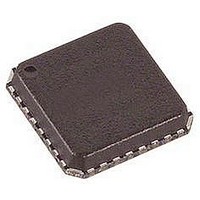
ADAU1381BCPZ Analog Devices Inc, ADAU1381BCPZ Datasheet - Page 35

ADAU1381BCPZ
Manufacturer Part Number
ADAU1381BCPZ
Description
IC AUDIO CODEC STEREO LN 32LFCSP
Manufacturer
Analog Devices Inc
Type
Stereo Audior
Datasheet
1.ADAU1381BCBZ-RL.pdf
(84 pages)
Specifications of ADAU1381BCPZ
Data Interface
Serial, SPI™
Resolution (bits)
24 b
Number Of Adcs / Dacs
2 / 2
Sigma Delta
No
S/n Ratio, Adcs / Dacs (db) Typ
97 / 100
Dynamic Range, Adcs / Dacs (db) Typ
96.5 / 100
Voltage - Supply, Analog
1.8 V ~ 3.65 V
Voltage - Supply, Digital
1.63 V ~ 3.65 V
Operating Temperature
-25°C ~ 85°C
Mounting Type
Surface Mount
Package / Case
32-VFQFN, CSP Exposed Pad
Audio Codec Type
Stereo
No. Of Adcs
2
No. Of Dacs
2
No. Of Input Channels
3
No. Of Output Channels
3
Adc / Dac Resolution
24bit
Adcs / Dacs Signal To Noise Ratio
100dB
Lead Free Status / RoHS Status
Lead free / RoHS Compliant
I
Figure 40 shows the timing of a single-word write operation.
Every ninth clock pulse, the ADAU1381 issues an acknowledge
by pulling SDA low.
Figure 41 shows the timing of a burst mode write sequence.
This figure shows an example where the target destination
registers are two bytes. The ADAU1381 knows to increment its
subaddress register every two bytes because the requested
subaddress corresponds to a register or memory area with a
2-byte word length.
The timing of a single-word read operation is shown in Figure 42.
Note that the first R/ W bit is 0, indicating a write operation. This is
because the subaddress still needs to be written to set up the
internal address. After the ADAU1381 acknowledges the receipt
2
C Read and Write Operations
S = START BIT, P = STOP BIT, AS = ACKNOWLEDGE BY SLAVE.
SHOWS AN N-WORD WRITE, WHERE EACH WORD HAS TWO BYTES. (OTHER WORD LENGTHS ARE POSSIBLE, RANGING FROM ONE TO FIVE BYTES.)
S = START BIT, P = STOP BIT, AM = ACKNOWLEDGE BY MASTER, AS = ACKNOWLEDGE BY SLAVE.
SHOWS A ONE-WORD READ, WHERE EACH WORD HAS N BYTES.
S = START BIT, P = STOP BIT, AM = ACKNOWLEDGE BY MASTER, AS = ACKNOWLEDGE BY SLAVE.
SHOWS AN N-WORD READ, WHERE EACH WORD HAS TWO BYTES. (OTHER WORD LENGTHS ARE POSSIBLE, RANGING FROM ONE TO FIVE BYTES.)
S
S
S
S = START BIT, P = STOP BIT, AS = ACKNOWLEDGE BY SLAVE.
SHOWS A ONE-WORD WRITE, WHERE EACH WORD HAS N BYTES.
S
ADDRESS,
ADDRESS,
CHIP ADDRESS,
CHIP ADDRESS,
R/W = 0
R/W = 0
CHIP
CHIP
R/W = 0
R/W = 0
AS
AS
SUBADDRESS,
SUBADDRESS,
AS
HIGH BYTE
HIGH BYTE
AS
SUBADDRESS,
HIGH BYTE
SUBADDRESS,
HIGH BYTE
AS
AS
SUBADDRESS,
SUBADDRESS,
LOW BYTE
LOW BYTE
AS
SUBADDRESS,
AS
LOW BYTE
Figure 40. Single-Word I
Figure 42. Single-Word I
Figure 41. Burst Mode I
Figure 43. Burst Mode I
AS
AS
SUBADDRESS,
LOW BYTE
DATA-WORD 1,
BYTE 1
S
AS
ADDRESS,
Rev. B | Page 35 of 84
R/W = 1
S
CHIP
AS
DATA-WORD 1,
CHIP ADDRESS,
AS
BYTE 2
R/W = 1
AS
2
2
2
C Write Sequence
2
C Read Sequence
C Write Sequence
C Read Sequence
BYTE 1
DATA-WORD 1,
DATA
AS
of the subaddress, the master must issue a repeated start command
followed by the chip address byte with the R/ W bit set to 1 (read).
This causes the ADAU1381 SDA to reverse and begin driving
data back to the master. The master then responds every ninth
pulse with an acknowledge pulse to the ADAU1381.
Figure 43 shows the timing of a burst mode read sequence. This
figure shows an example where the target read registers are two
bytes. The ADAU1381 increments its subaddress every two bytes
because the requested subaddress corresponds to a register or
memory area with word lengths of two bytes. Other address
ranges may have a variety of word lengths ranging from one to
five bytes. The ADAU1381 always decodes the subaddress and
sets the auto-increment circuit so that the address increments
after the appropriate number of bytes.
DATA-WORD 2,
BYTE 1
AS
BYTE 1
BYTE 1
DATA
AS
AS
AM
DATA-WORD 2,
DATA-WORD 1,
BYTE 2
BYTE 2
BYTE 2
AM
DATA
BYTE 2
AM
AS
DATA
AS
...
...
DATA-WORD N,
DATA-WORD N,
AM
...
BYTE 1
BYTE 1
...
BYTE N
DATA
AM
AS
DATA-WORD N,
DATA-WORD N,
BYTE N
DATA
BYTE 2
BYTE 2
AS
AM
AS
AM
ADAU1381
P
P
P
P


