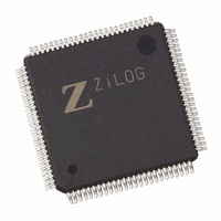
EZ80190AZ050SG Zilog, EZ80190AZ050SG Datasheet - Page 55

EZ80190AZ050SG
Manufacturer Part Number
EZ80190AZ050SG
Description
IC WEBSERVER 8 BIT 50MHZ 100LQFP
Manufacturer
Zilog
Datasheet
1.EZ80190AZ050SG.pdf
(221 pages)
Specifications of EZ80190AZ050SG
Processor Type
eZ80
Features
High Speed, Single-Cycle Instruction-Fetch
Speed
50MHz
Voltage
3.3V
Mounting Type
Surface Mount
Package / Case
100-LQFP
Processor Series
EZ80190x
Core
eZ80
Data Bus Width
8 bit
Program Memory Type
ROMLess
Data Ram Size
8 KB
Interface Type
I2C, IrDA, SPI, UART
Maximum Clock Frequency
50 MHz
Number Of Programmable I/os
32
Number Of Timers
6
Operating Supply Voltage
3 V to 3.6 V
Maximum Operating Temperature
+ 105 C
Mounting Style
SMD/SMT
Minimum Operating Temperature
- 40 C
Lead Free Status / RoHS Status
Lead free / RoHS Compliant
Other names
269-3866
EZ80190AZ050SG
EZ80190AZ050SG
Available stocks
Company
Part Number
Manufacturer
Quantity
Price
Company:
Part Number:
EZ80190AZ050SG
Manufacturer:
ZiLOG
Quantity:
135
- Current page: 55 of 221
- Download datasheet (4Mb)
PS006614-1208
GPIO Mode 6—
falling edge on the pin cause an interrupt request to be sent to the CPU. Writing a 1 to the
Port x Data register bit position resets the corresponding interrupt request. Writing a 0 pro-
duces no effect. The programmer must set the Port x Data register before entering the dual-
edge-triggered interrupt mode.
GPIO Mode 7—
alternate functions assigned to the pin. For example, the alternate mode function for PC7
is RI1. When GPIO Mode 7 is enabled, the pin output data and pin tristate control come
from the alternate function's data output and tristate control, respectively. The value in the
Port x Data register produces no effect on operation.
For Ports A and B, which do not feature alternate I/O functions, selecting GPIO Mode 7
results in a configuration of the pins for input from the pin and high-impedance output as
in GPIO Mode 2.
GPIO Mode 8—
rupt request is generated when the level at the pin is the same as the level stored in the
Port x Data register. The port pin value is sampled by the system clock. The input pin must
be held at the selected interrupt level for a minimum of 2 clock periods to initiate an inter-
rupt. The interrupt request remains active as long as this condition is maintained at the
external source.
GPIO Mode 9—
value in the Port x Data register determines if a positive or negative edge causes an inter-
rupt request. A 0 in the Port x Data register bit sets the selected pin to generate an interrupt
request for falling edges. A 1 in the Port x Data register bit sets the selected pin to generate
an interrupt request for rising edges. The interrupt request remains active until a 1 is writ-
ten to the Port x Data register bit’s corresponding interrupt request. Writing a 0 produces
no effect on operation. The programmer must set the Port x Data register before entering
the single-edge-triggered interrupt mode.
A simplified block diagram of a GPIO port pin is displayed in
The bit enables a dual-edge-triggered interrupt mode. Both a rising and a
For Ports C and D, the port pin is configured to pass control over to the
The port pin is configured for level-sensitive interrupt modes. An inter-
The port pin is configured for single-edge-triggered interrupt mode. The
Figure 7
General-Purpose Input/Output
Product Specification
on page 46.
eZ80190
45
Related parts for EZ80190AZ050SG
Image
Part Number
Description
Manufacturer
Datasheet
Request
R

Part Number:
Description:
Communication Controllers, ZILOG INTELLIGENT PERIPHERAL CONTROLLER (ZIP)
Manufacturer:
Zilog, Inc.
Datasheet:

Part Number:
Description:
KIT DEV FOR Z8 ENCORE 16K TO 64K
Manufacturer:
Zilog
Datasheet:

Part Number:
Description:
KIT DEV Z8 ENCORE XP 28-PIN
Manufacturer:
Zilog
Datasheet:

Part Number:
Description:
DEV KIT FOR Z8 ENCORE 8K/4K
Manufacturer:
Zilog
Datasheet:

Part Number:
Description:
KIT DEV Z8 ENCORE XP 28-PIN
Manufacturer:
Zilog
Datasheet:

Part Number:
Description:
DEV KIT FOR Z8 ENCORE 4K TO 8K
Manufacturer:
Zilog
Datasheet:

Part Number:
Description:
CMOS Z8 microcontroller. ROM 16 Kbytes, RAM 256 bytes, speed 16 MHz, 32 lines I/O, 3.0V to 5.5V
Manufacturer:
Zilog, Inc.
Datasheet:

Part Number:
Description:
Low-cost microcontroller. 512 bytes ROM, 61 bytes RAM, 8 MHz
Manufacturer:
Zilog, Inc.
Datasheet:

Part Number:
Description:
Z8 4K OTP Microcontroller
Manufacturer:
Zilog, Inc.
Datasheet:

Part Number:
Description:
CMOS SUPER8 ROMLESS MCU
Manufacturer:
Zilog, Inc.
Datasheet:

Part Number:
Description:
SL1866 CMOSZ8 OTP Microcontroller
Manufacturer:
Zilog, Inc.
Datasheet:

Part Number:
Description:
SL1866 CMOSZ8 OTP Microcontroller
Manufacturer:
Zilog, Inc.
Datasheet:

Part Number:
Description:
OTP (KB) = 1, RAM = 125, Speed = 12, I/O = 14, 8-bit Timers = 2, Comm Interfaces Other Features = Por, LV Protect, Voltage = 4.5-5.5V
Manufacturer:
Zilog, Inc.
Datasheet:

Part Number:
Description:
Manufacturer:
Zilog, Inc.
Datasheet:


