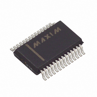
MAX1403EAI+ Maxim Integrated Products, MAX1403EAI+ Datasheet - Page 29

MAX1403EAI+
Manufacturer Part Number
MAX1403EAI+
Description
IC ADC 18BIT LP 28-SSOP
Manufacturer
Maxim Integrated Products
Datasheet
1.MAX1403EAI.pdf
(36 pages)
Specifications of MAX1403EAI+
Number Of Bits
18
Sampling Rate (per Second)
480
Data Interface
QSPI™, Serial, SPI™
Number Of Converters
1
Power Dissipation (max)
21.45mW
Voltage Supply Source
Analog and Digital
Operating Temperature
-40°C ~ 85°C
Mounting Type
Surface Mount
Package / Case
28-SSOP
Number Of Adc Inputs
5
Architecture
Delta-Sigma
Conversion Rate
4.8 KSPs
Resolution
18 bit
Input Type
Voltage
Interface Type
Serial
Voltage Reference
External
Supply Voltage (max)
3 V
Maximum Power Dissipation
21.45 mW
Maximum Operating Temperature
+ 85 C
Mounting Style
SMD/SMT
Input Signal Type
Pseudo-Differential, Differential
Minimum Operating Temperature
- 40 C
Lead Free Status / RoHS Status
Lead free / RoHS Compliant
The on-chip digital filter processes the 1-bit data
stream from the modulator using a SINC
ter. The SINC filters are conceptually simple, efficient,
and extremely flexible, especially where variable reso-
lution and data rates are required. Also, the filter notch
positions are easily controlled since they are directly
related to the output data rate (1 / data word period).
The SINC
while retaining the same frequency response notches
as the default SINC
faster at the expense of resolution and quantization
noise. The SINC
With 60Hz notches (60Hz data rate), the settling time
would be 1 / 60Hz or 16.7ms, whereas the SINC
would settle in 3 / 60Hz or 50ms. Toggle between these
filter responses using the FAST bit in the global setup
register. Use SINC
to SINC
the SINC
The DRDY signal will go false and will be reasserted
when valid data is available, a minimum of three data-
word periods later.
The digital filter can be bypassed by setting the MDOUT
bit in the global setup register. When MDOUT = 1, the
raw output of the modulator is directly available at DOUT.
The MAX1403 digital filter implements both a SINC
(sinx/x) and SINC
transfer function for the SINC
cascaded SINC
and in the frequency domain by:
where N, the decimation factor, is the ratio of the modu-
lator frequency f
Figure 10 shows the filter frequency response. The
SINC
first notch frequency. This results in a cutoff frequency
3
characteristic cutoff frequency is 0.262 times the
3
mode when full accuracy is required. Switch from
1
1
to SINC
function results in a faster settling response
H(f)
H(z)
1
M
1
filters described in the z-domain by:
3
filter settles in one data word period.
=
3
to the output frequency f
______________________________________________________________________________________
1
(sinx/x)
3
mode by resetting the FAST bit low.
=
mode for faster settling and switch
filter. This allows the filter to settle
N
1
N
1
⋅
+3V, 18-Bit, Low-Power, Multichannel,
⋅
3
Filter Characteristics
sin N
lowpass filter function. The
sin
1
3
1 – z
function is that of three
−
π
π
z
f
M
f
f
M
f
−
−
Oversampling (Sigma-Delta) ADC
N
1
Digital Filter
3
3
3
N
or SINC
.
3
filter
1
fil-
1
of 15.72Hz for a first filter notch frequency of 60Hz. The
response shown in Figure 10 is repeated at either side
of the digital filter’s sample frequency (f
side of the related harmonics (2f
The response of the SINC
SINC
The output data rate for the digital filter corresponds
with the positioning of the first notch of the filter’s fre-
quency response. Therefore, for the plot of Figure 10
where the first notch of the filter is at 60Hz, the output
data rate is 60Hz. The notches of this (sinx/x)
repeated at multiples of the first notch frequency. The
SINC
100dB at these notches.
Determine the cutoff frequency of the digital filter by the
value loaded into CLK, X2CLK, MF1, MF0, FS1, and FS0
in the global setup register. Programming a different
cutoff frequency with FS0 and FS1 does not alter the
profile of the filter response; it changes the frequency of
the notches. For example, Figure 11 shows a cutoff fre-
quency of 13.1Hz and a first notch frequency of 50Hz.
For step changes at the input, a settling time must be
allowed before valid data can be read. The settling time
depends upon the output data rate chosen for the filter.
The settling time of the SINC
input can be up to four-times the output data period.
For a synchronized step input (using the FSYNC func-
tion or the internal scanning logic), the settling time is
three-times the output data period.
Figure 10. Frequency Response of the SINC
60Hz)
1
3
(averaging filter) filter but with a sharper rolloff.
filter provides an attenuation of better than
-100
-120
-140
-160
-20
-40
-60
-80
0
0
20
40 60 80
FREQUENCY (Hz)
3
100 120 140 160 180 200
filter is similar to that of a
3
filter to a full-scale step
f
MF1, 0 = 0
FS1, 0 = 1
f
CLKIN
N
M
= 60Hz
, 3f
= 2.4576MHz
M
, . . .).
3
M
Filter (Notch at
) and at either
3
filter are
29


