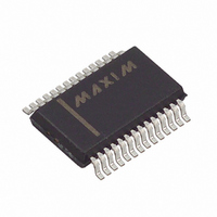
MAX1403EAI+ Maxim Integrated Products, MAX1403EAI+ Datasheet - Page 15

MAX1403EAI+
Manufacturer Part Number
MAX1403EAI+
Description
IC ADC 18BIT LP 28-SSOP
Manufacturer
Maxim Integrated Products
Datasheet
1.MAX1403EAI.pdf
(36 pages)
Specifications of MAX1403EAI+
Number Of Bits
18
Sampling Rate (per Second)
480
Data Interface
QSPI™, Serial, SPI™
Number Of Converters
1
Power Dissipation (max)
21.45mW
Voltage Supply Source
Analog and Digital
Operating Temperature
-40°C ~ 85°C
Mounting Type
Surface Mount
Package / Case
28-SSOP
Number Of Adc Inputs
5
Architecture
Delta-Sigma
Conversion Rate
4.8 KSPs
Resolution
18 bit
Input Type
Voltage
Interface Type
Serial
Voltage Reference
External
Supply Voltage (max)
3 V
Maximum Power Dissipation
21.45 mW
Maximum Operating Temperature
+ 85 C
Mounting Style
SMD/SMT
Input Signal Type
Pseudo-Differential, Differential
Minimum Operating Temperature
- 40 C
Lead Free Status / RoHS Status
Lead free / RoHS Compliant
The serial interface can be operated with the clock idling
either high or low. This is compatible with Motorola’s SPI
interface operated in CPOL = 1, CPHA = 1 mode or
CPOL = 0, CPHA = 1 mode. The clock polarity is deter-
mined by the state of SCLK at the falling edge of CS.
Ensure that the setup times t
ed. If CS is connected to ground, resulting in no falling
edge on CS, SCLK must idle high (CPOL = 1, CPHA = 1).
The data-ready signal indicates that new data may be
read from the 24-bit data register. After the end of a suc-
cessful data register read, the data-ready signal
becomes false. If a new measurement completes before
the data is read, the data-ready signal becomes false.
The data-ready signal becomes true again when new
data is available in the data register.
The MAX1403 provides two methods of monitoring the
data-ready signal. INT provides a hardware solution
(active low when data is ready to be accessed), while
the DRDY bit in the COMM register provides a software
solution (active high).
Read data as soon as possible once data-ready
becomes true. This becomes increasingly important for
faster measurement rates. If the data read is delayed
significantly, a collision may result. A collision occurs
when a new measurement completes during a data-
register read operation. After a collision, information in
the data register is invalid. The failed read operation
must be completed even though the data is invalid.
Reset the serial interface by clocking in 32 1s.
Resetting the interface does not affect the internal reg-
isters.
If continuous data output mode is in use, clock in eight
0s followed by 32 1s. More than 32 1s may be clocked
in, since a leading 0 is used as the start bit for all oper-
ations.
When scanning the input channels (SCAN = 1), the ser-
ial interface allows the data register to be read repeat-
edly without requiring a write to the COMM register.
Communications Register
Name
Defaults
FUNCTION
Data-Ready Signal (DRDY bit true or I I N N T T = low)
______________________________________________________________________________________
First Bit (MSB)
0/DRDY
DATA
Continuous Data Output Mode
RDY
+3V, 18-Bit, Low-Power, Multichannel,
0
4
/t
12
Selecting Clock Polarity
Resetting the Interface
and t
RS2
Oversampling (Sigma-Delta) ADC
0
5
REGISTER SELECT BITS
/t
13
are not violat-
RS1
0
RS0
The initial COMM write (01111000) is followed by 24
clocks (DIN = high) to read the 24-bit data register.
Once the data register has been read, it can be read
again after the next conversion by writing another 24
clocks (DIN = high). Terminate the continuous data out-
put mode by writing to the COMM register with any
valid access.
Single-bit, raw modulator data is available at DOUT for
custom filtering when MDOUT = 1. INT provides a mod-
ulator clock for data synchronization. Data is valid on
the falling edge of INT. Write operations can still be
performed; however, read operations are disabled.
After MDOUT is returned to 0, valid data is accessed
by the normal serial-interface read operation.
0/DRDY: (Default = 0) Data Ready Bit. On a write, this
bit must be reset to 0 to signal the start of the Com-
munications Register data word. On a read, a 1 in this
location (0/DRDY) signifies that valid data is available in
the data register. This bit is reset after the data register
is read or, if data is not read, 0/DRDY will go low at the
end of the next measurement.
RS2, RS1, RS0: (Default = 0, 0, 0) Register Select
Bits. These bits select the register to be accessed
(Table 1).
R/W: (Default = 0) Read/Write Bit. When set high, the
selected register is read; when R/W = 0, the selected
register is written.
RESET: (Default = 0) Software Reset Bit. Setting this
bit high causes the part to be reset to its default power-
up condition (RESET = 0).
STDBY: (Default = 0) Standby Power-Down Bit. Setting
the STDBY bit places the part in “standby” condition,
shutting down everything except the serial interface
and the CLK oscillator.
FSYNC: (Default = 0) Filter Sync Bit. When FSYNC = 0,
conversions are automatically performed at a data rate
determined by CLK, FS1, FS0, MF1, and MF0 bits.
When FSYNC = 1, the digital filter and analog modulator
0
R/W
0
Modulator Data Output (MDOUT = 1)
RESET
0
Communications Register
On-Chip Registers
STDBY
0
FSYNC
(LSB)
0
15


