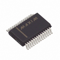
MAX1403EAI+ Maxim Integrated Products, MAX1403EAI+ Datasheet - Page 12

MAX1403EAI+
Manufacturer Part Number
MAX1403EAI+
Description
IC ADC 18BIT LP 28-SSOP
Manufacturer
Maxim Integrated Products
Datasheet
1.MAX1403EAI.pdf
(36 pages)
Specifications of MAX1403EAI+
Number Of Bits
18
Sampling Rate (per Second)
480
Data Interface
QSPI™, Serial, SPI™
Number Of Converters
1
Power Dissipation (max)
21.45mW
Voltage Supply Source
Analog and Digital
Operating Temperature
-40°C ~ 85°C
Mounting Type
Surface Mount
Package / Case
28-SSOP
Number Of Adc Inputs
5
Architecture
Delta-Sigma
Conversion Rate
4.8 KSPs
Resolution
18 bit
Input Type
Voltage
Interface Type
Serial
Voltage Reference
External
Supply Voltage (max)
3 V
Maximum Power Dissipation
21.45 mW
Maximum Operating Temperature
+ 85 C
Mounting Style
SMD/SMT
Input Signal Type
Pseudo-Differential, Differential
Minimum Operating Temperature
- 40 C
Lead Free Status / RoHS Status
Lead free / RoHS Compliant
+3V, 18-Bit, Low-Power, Multichannel,
Oversampling (Sigma-Delta) ADC
12
PIN
19
20
21
22
23
24
25
26
27
28
______________________________________________________________________________________
CALOFF+
CALOFF-
REFIN+
REFIN-
NAME
DGND
DOUT
SCLK
V
DIN
INT
DD
Negative Differential Reference Input. Bias REFIN- between V+ and AGND, provided that REFIN+ is more
positive than REFIN-.
Positive Differential Reference Input. Bias REFIN+ between V+ and AGND, provided that REFIN+ is more
positive than REFIN-.
Negative Offset Calibration Input. Used for system offset calibration. It forms the negative input of a fully
differential input pair with CALOFF+. Normally these inputs are connected to zero-reference voltages in
the system. When system offset calibration is not required and the auto-sequence mode is used, the
CALOFF+/CALOFF- input pair provides an additional fully differential input channel.
Positive Offset Calibration Input. Used for system offset calibration. It forms the positive input of a fully
differential input pair with CALOFF-. Normally these inputs are connected to zero-reference voltages in the
system. When system offset calibration is not required and the auto-sequence mode is used, the
CALOFF+/CALOFF- input pair provides an additional fully differential input channel.
Digital Ground. Reference point for digital circuitry.
Digital Supply Voltage (+2.7V to +3.6V)
Interrupt Output. A logic low indicates that a new output word is available from the data register. INT
returns high upon completion of a full output word read operation. INT also returns high for short periods
(determined by the filter and clock control bits) if no data read has taken place. A logic high indicates
internal activity, and a read operation should not be attempted under this condition. INT can also provide
a strobe to indicate valid data at DOUT (MDOUT = 1).
Serial Data Output. DOUT outputs data from the internal shift register containing information from the
Communications Register, Global Setup Registers, Transfer Function Registers, or Data Register. DOUT
can also provide the digital bit stream directly from the Σ-∆ modulator (MDOUT = 1).
Serial Data Input. Data on DIN is written to the input shift register and later transferred to the
Communications Register, Global Setup Registers, Special Function Register, or Transfer Function
Registers, depending on the register selection bits in the Communications Register.
Serial Clock Input. Apply an external serial clock to transfer data to and from the MAX1403. This serial
clock can be continuous, with data transmitted in a train of pulses, or intermittently. If CS is used to frame
the data transfer, then SCLK may idle high or low between conversions and CS determines the desired
active clock edge (see Selecting Clock Polarity). If CS is tied permanently low, SCLK must idle high
between data transfers.
FUNCTION
Pin Description (continued)


