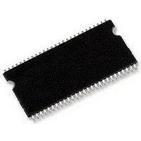
MT48LC16M16A2P-7E:D Micron Technology Inc, MT48LC16M16A2P-7E:D Datasheet - Page 41

MT48LC16M16A2P-7E:D
Manufacturer Part Number
MT48LC16M16A2P-7E:D
Description
SDRAM 256MB, SMD, 48LC16, TSOP54
Manufacturer
Micron Technology Inc
Type
SDRAMr
Series
-r
Specifications of MT48LC16M16A2P-7E:D
Organization
16Mx16
Density
256Mb
Address Bus
15b
Access Time (max)
5.4ns
Maximum Clock Rate
143MHz
Operating Supply Voltage (typ)
3.3V
Package Type
TSOP-II
Operating Temp Range
0C to 70C
Operating Supply Voltage (max)
3.6V
Operating Supply Voltage (min)
3V
Supply Current
135mA
Pin Count
54
Mounting
Surface Mount
Operating Temperature Classification
Commercial
Access Time
RoHS Compliant
Memory Case Style
TSOP
No. Of Pins
54
Operating Temperature Range
0°C To +70°C
Operating Temperature Max
70°C
Operating Temperature Min
0°C
Package / Case
TSOP
Memory Type
DRAM - Synchronous
Memory Configuration
4 BLK (4M X 16)
Interface Type
LVTTL
Rohs Compliant
Yes
Format - Memory
RAM
Memory Size
256M (16Mx16)
Speed
133MHz
Interface
Parallel
Voltage - Supply
3 V ~ 3.6 V
Operating Temperature
0°C ~ 70°C
Lead Free Status / RoHS Status
Compliant
Lead Free Status / RoHS Status
Compliant
Available stocks
Company
Part Number
Manufacturer
Quantity
Price
Company:
Part Number:
MT48LC16M16A2P-7E:D
Manufacturer:
MICRON
Quantity:
5 520
Company:
Part Number:
MT48LC16M16A2P-7E:D TR
Manufacturer:
MICRON
Quantity:
11 200
Company:
Part Number:
MT48LC16M16A2P-7E:D TR
Manufacturer:
AVAGO
Quantity:
6 700
PDF: 09005aef80725c0b/Source: 09005aef806fc13c
64MSDRAM_2.fm - Rev. M 10/07 EN
10. For a READ without auto precharge interrupted by a READ (with or without auto pre-
11. For a READ without auto precharge interrupted by a WRITE (with or without auto pre-
12. For a WRITE without auto precharge interrupted by a READ (with or without auto pre-
13. For a WRITE without auto precharge interrupted by a WRITE (with or without auto pre-
14. For a READ with auto precharge interrupted by a READ (with or without auto precharge),
15. For a READ with auto precharge interrupted by a WRITE (with or without auto precharge),
16. For a WRITE with auto precharge interrupted by a READ (with or without auto precharge),
17. For a WRITE with auto precharge interrupted by a WRITE (with or without auto precharge),
6. All states and sequences not shown are illegal or reserved.
7. READs or WRITEs to bank m listed in the Command (Action) column include READs or
8. Concurrent Auto precharge: Bank n will initiate the auto precharge command when its
9. Burst in bank n continues as initiated.
WRITEs with auto precharge enabled and READs or WRITEs with auto precharge disabled.
burst has been interrupted by bank m’s burst.
charge), the READ to bank m will interrupt the READ on bank n, CL later (Figure 12 on
page 23).
charge), the WRITE to bank m will interrupt the READ on bank n when registered
(Figures 14 and 15 on page 25). DQM should be used one clock prior to the WRITE com-
mand to prevent bus contention.
charge), the READ to bank m will interrupt the WRITE on bank n when registered (Figure 22
on page 30), with the data-out appearing CL later. The last valid WRITE to bank n will be
data-in registered one clock prior to the READ to bank m.
charge), the WRITE to bank m will interrupt the WRITE on bank n when registered
(Figure 20 on page 29). The last valid WRITE to bank n will be data-in registered one clock
prior to the READ to bank m.
the READ to bank m will interrupt the READ on bank n, CL later. The precharge to bank n
will begin when the READ to bank m is registered (Figure 29 on page 35).
the WRITE to bank m will interrupt the READ on bank n when registered. DQM should be
used two clocks prior to the WRITE command to prevent bus contention. The precharge to
bank n will begin when the WRITE to bank m is registered (Figure 30 on page 36).
the READ to bank m will interrupt the WRITE on bank n when registered, with the data-out
appearing CL later. The precharge to bank n will begin after
when the READ to bank m is registered. The last valid WRITE to bank n will be data-in regis-
tered one clock prior to the READ to bank m (Figure 31 on page 36).
the WRITE to bank m will interrupt the WRITE on bank n when registered. The precharge to
bank n will begin after
tered. The last valid WRITE to bank n will be data registered one clock prior to the WRITE to
bank m (Figure 32 on page 37).
t
WR is met, where
41
Micron Technology, Inc., reserves the right to change products or specifications without notice.
t
WR begins when the WRITE to bank m is regis-
64Mb: x4, x8, x16 SDRAM
t
WR is met, where
©2000 Micron Technology, Inc. All rights reserved.
Commands
t
WR begins


