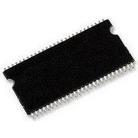
MT48LC16M16A2P-7E:D Micron Technology Inc, MT48LC16M16A2P-7E:D Datasheet - Page 20

MT48LC16M16A2P-7E:D
Manufacturer Part Number
MT48LC16M16A2P-7E:D
Description
SDRAM 256MB, SMD, 48LC16, TSOP54
Manufacturer
Micron Technology Inc
Type
SDRAMr
Series
-r
Specifications of MT48LC16M16A2P-7E:D
Organization
16Mx16
Density
256Mb
Address Bus
15b
Access Time (max)
5.4ns
Maximum Clock Rate
143MHz
Operating Supply Voltage (typ)
3.3V
Package Type
TSOP-II
Operating Temp Range
0C to 70C
Operating Supply Voltage (max)
3.6V
Operating Supply Voltage (min)
3V
Supply Current
135mA
Pin Count
54
Mounting
Surface Mount
Operating Temperature Classification
Commercial
Access Time
RoHS Compliant
Memory Case Style
TSOP
No. Of Pins
54
Operating Temperature Range
0°C To +70°C
Operating Temperature Max
70°C
Operating Temperature Min
0°C
Package / Case
TSOP
Memory Type
DRAM - Synchronous
Memory Configuration
4 BLK (4M X 16)
Interface Type
LVTTL
Rohs Compliant
Yes
Format - Memory
RAM
Memory Size
256M (16Mx16)
Speed
133MHz
Interface
Parallel
Voltage - Supply
3 V ~ 3.6 V
Operating Temperature
0°C ~ 70°C
Lead Free Status / RoHS Status
Compliant
Lead Free Status / RoHS Status
Compliant
Available stocks
Company
Part Number
Manufacturer
Quantity
Price
Company:
Part Number:
MT48LC16M16A2P-7E:D
Manufacturer:
MICRON
Quantity:
5 520
Company:
Part Number:
MT48LC16M16A2P-7E:D TR
Manufacturer:
MICRON
Quantity:
11 200
Company:
Part Number:
MT48LC16M16A2P-7E:D TR
Manufacturer:
AVAGO
Quantity:
6 700
Operation
Bank/Row Activation
Figure 8:
PDF: 09005aef80725c0b/Source: 09005aef806fc13c
64MSDRAM_2.fm - Rev. M 10/07 EN
Activating a Specific Row in a Specific Bank
Upon exiting the self refresh mode, AUTO REFRESH commands must be issued every
15.625µs or less, as both SELF REFRESH and AUTO REFRESH utilize the row refresh
counter.
Before any READ or WRITE commands can be issued to a bank within the SDRAM, a row
in that bank must be “opened.” This is accomplished via the ACTIVE command, which
selects both the bank and the row to be activated (see Figure 8).
After opening a row (issuing an ACTIVE command), a READ or WRITE command may be
issued to that row, subject to the
the clock period and rounded up to the next whole number to determine the earliest
clock edge after the ACTIVE command on which a READ or WRITE command can be
entered. For example, a
results in 2.5 clocks, rounded to 3. This is reflected in Figure 9 on page 21, which covers
any case where 2 <
specification limits from time units to clock cycles).
A subsequent ACTIVE command to a different row in the same bank can only be issued
after the previous active row has been “closed” (precharged). The minimum time
interval between successive ACTIVE commands to the same bank is defined by
A subsequent ACTIVE command to another bank can be issued while the first bank is
being accessed, which results in a reduction of total row-access overhead. The
minimum time interval between successive ACTIVE commands to different banks is
defined by
A0–A10, A11
BA0, BA1
RAS#
CAS#
WE#
CKE
CLK
CS#
t
RRD.
HIGH
t
RCD (MIN)/
t
RCD specification of 20ns with a 125 MHz clock (8ns period)
ADDRESS
ADDRESS
BANK
ROW
20
t
t
CK ≤ 3. (The same procedure is used to convert other
DON’T CARE
RCD specification.
Micron Technology, Inc., reserves the right to change products or specifications without notice.
t
RCD (MIN) should be divided by
64Mb: x4, x8, x16 SDRAM
©2000 Micron Technology, Inc. All rights reserved.
Commands
t
RC.


