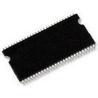
MT48LC16M16A2P-7E:D Micron Technology Inc, MT48LC16M16A2P-7E:D Datasheet - Page 25

MT48LC16M16A2P-7E:D
Manufacturer Part Number
MT48LC16M16A2P-7E:D
Description
SDRAM 256MB, SMD, 48LC16, TSOP54
Manufacturer
Micron Technology Inc
Type
SDRAMr
Series
-r
Specifications of MT48LC16M16A2P-7E:D
Organization
16Mx16
Density
256Mb
Address Bus
15b
Access Time (max)
5.4ns
Maximum Clock Rate
143MHz
Operating Supply Voltage (typ)
3.3V
Package Type
TSOP-II
Operating Temp Range
0C to 70C
Operating Supply Voltage (max)
3.6V
Operating Supply Voltage (min)
3V
Supply Current
135mA
Pin Count
54
Mounting
Surface Mount
Operating Temperature Classification
Commercial
Access Time
RoHS Compliant
Memory Case Style
TSOP
No. Of Pins
54
Operating Temperature Range
0°C To +70°C
Operating Temperature Max
70°C
Operating Temperature Min
0°C
Package / Case
TSOP
Memory Type
DRAM - Synchronous
Memory Configuration
4 BLK (4M X 16)
Interface Type
LVTTL
Rohs Compliant
Yes
Format - Memory
RAM
Memory Size
256M (16Mx16)
Speed
133MHz
Interface
Parallel
Voltage - Supply
3 V ~ 3.6 V
Operating Temperature
0°C ~ 70°C
Lead Free Status / RoHS Status
Compliant
Lead Free Status / RoHS Status
Compliant
Available stocks
Company
Part Number
Manufacturer
Quantity
Price
Company:
Part Number:
MT48LC16M16A2P-7E:D
Manufacturer:
MICRON
Quantity:
5 520
Company:
Part Number:
MT48LC16M16A2P-7E:D TR
Manufacturer:
MICRON
Quantity:
11 200
Company:
Part Number:
MT48LC16M16A2P-7E:D TR
Manufacturer:
AVAGO
Quantity:
6 700
Figure 14:
Figure 15:
PDF: 09005aef80725c0b/Source: 09005aef806fc13c
64MSDRAM_2.fm - Rev. M 10/07 EN
READ-to-WRITE
READ-to-WRITE With Extra Clock Cycle
Note:
Note:
The DQM signal must be de-asserted prior to the WRITE command (DQM latency is
zero clocks for input buffers) to ensure that the written data is not masked. Figure 14
shows the case where the clock frequency allows for bus contention to be avoided
without adding a NOP cycle, and Figure 15 shows the case where the additional NOP is
needed.
COMMAND
COMMAND
ADDRESS
ADDRESS
CL = 3 is used for illustration. The READ command may be to any bank, and the WRITE
command may be to any bank. If a burst of one is used, then DQM is not required.
CL = 3 is used for illustration. The READ command may be to any bank, and the WRITE
command may be to any bank.
DQM
DQM
CLK
CLK
DQ
DQ
BANK,
COL n
T0
BANK,
T0
COL n
READ
READ
TRANSITIONING DATA
T1
T1
NOP
NOP
25
T2
T2
TRANSITIONING DATA
NOP
NOP
Micron Technology, Inc., reserves the right to change products or specifications without notice.
T3
T3
NOP
NOP
D
t HZ
OUT
t HZ
D
t CK
OUT
n
n
DON’T CARE
T4
BANK,
T4
COL b
WRITE
NOP
D
IN
b
t
DS
64Mb: x4, x8, x16 SDRAM
DON’T CARE
T5
BANK,
COL b
WRITE
D
IN
b
t
DS
©2000 Micron Technology, Inc. All rights reserved.
Commands


