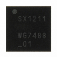
SX1211I084TRT Semtech, SX1211I084TRT Datasheet - Page 8

SX1211I084TRT
Manufacturer Part Number
SX1211I084TRT
Description
IC SNGL-CHIP TXRX 32-TQFN
Manufacturer
Semtech
Specifications of SX1211I084TRT
Frequency
860 ~ 960MHz
Data Rate - Maximum
200kbps
Modulation Or Protocol
FSK, OOK
Applications
AMR, ISM, Security and Access
Power - Output
12.5dBm
Sensitivity
-113dBm
Voltage - Supply
2.1 V ~ 3.6 V
Current - Receiving
3mA
Current - Transmitting
25mA
Data Interface
PCB, Surface Mount
Antenna Connector
PCB, Surface Mount
Operating Temperature
-40°C ~ 85°C
Package / Case
32-TQFN
Operating Temperature (min)
-40C
Operating Temperature (max)
85C
Operating Temperature Classification
Industrial
Modulation Type
FSK/OOK
Package Type
TQFN EP
Operating Supply Voltage (min)
2.1V
Operating Supply Voltage (typ)
2.5/3.3V
Operating Supply Voltage (max)
3.6V
Lead Free Status / RoHS Status
Lead free / RoHS Compliant
Memory Size
-
Lead Free Status / Rohs Status
Compliant
Other names
SX1211I084TRT
Available stocks
Company
Part Number
Manufacturer
Quantity
Price
Company:
Part Number:
SX1211I084TRT
Manufacturer:
HITTITE
Quantity:
560
2. Electrical Characteristics
The SX1211 is a high performance radio frequency device. It satisfies:
It should thus be handled with all the necessary ESD precautions to avoid any permanent damage.
Stresses above the values listed below may cause permanent device failure. Exposure to absolute maximum
ratings for extended periods may affect device reliability.
Table 3: Absolute Maximum Ratings
Table 4: Operating Range
Conditions: Temp = 25 ° C, VDD = 3.3 V, crystal freq uency = 12.8 MHz, carrier frequency = 869 or 915 MHz,
modulation FSK, data rate = 25 kb/s, Fdev = 50 kHz, fc = 100 kHz, unless otherwise specified.
Table 5: Power Consumption Specification
Symbol
IDDSL
IDDST
IDDFS
IDDR
IDDT
(1)
(2)
Rev 7 – Sept 2
ADVANCED COMMUNICATIONS & SENSING
Guaranteed by design and characterization
Crystal Cload=10pF, C0=2.5pF, Rm=15 Ohms
2.1. ESD Notice
Class 2 of the JEDEC standard JESD22-A114-B (Human Body Model), except on pins 3-4-5-27-28-29-31
where it satisfies Class 1A.
Class III of the JEDEC standard JESD22-C101C (Charged Device Model) on all pins.
2.2. Absolute Maximum Ratings
2.3. Operating Range
2.4. Chip Specification
Symbol
VDDmr
Symbol
VDDop
Pmr
Tmr
Trop
ML
2.4.1. Power Consumption
nd
, 2008
Description
Supply current, Sleep mode
Supply current in standby
mode, CLKOUT disabled
Supply current in FS mode
Supply current in Rx mode
Supply current in Tx mode
Storage temperature
Supply voltage
Supply Voltage
Description
Temperature
Description
Input level
Input Level
Conditions
Crystal oscillator running
Frequency synthesizer
running
Output power = +10 dBm
Output power = 1dBm
Page 8 of 92
(1)
(2)
Min
Min
-0.3
-55
Min
2.1
-40
-
-
-
-
-
-
-
-
Typ
0.1
1.3
3.0
65
25
16
Max
125
Max
3.7
+85
3.6
0
0
Max
1.7
3.5
80
30
21
2
Unit
V
° C
dBm
www.semtech.com
dBm
Unit
SX1211
° C
V
Unit
µA
µA
mA
mA
mA
mA


