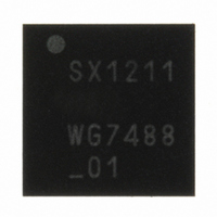
SX1211I084TRT Semtech, SX1211I084TRT Datasheet - Page 18

SX1211I084TRT
Manufacturer Part Number
SX1211I084TRT
Description
IC SNGL-CHIP TXRX 32-TQFN
Manufacturer
Semtech
Specifications of SX1211I084TRT
Frequency
860 ~ 960MHz
Data Rate - Maximum
200kbps
Modulation Or Protocol
FSK, OOK
Applications
AMR, ISM, Security and Access
Power - Output
12.5dBm
Sensitivity
-113dBm
Voltage - Supply
2.1 V ~ 3.6 V
Current - Receiving
3mA
Current - Transmitting
25mA
Data Interface
PCB, Surface Mount
Antenna Connector
PCB, Surface Mount
Operating Temperature
-40°C ~ 85°C
Package / Case
32-TQFN
Operating Temperature (min)
-40C
Operating Temperature (max)
85C
Operating Temperature Classification
Industrial
Modulation Type
FSK/OOK
Package Type
TQFN EP
Operating Supply Voltage (min)
2.1V
Operating Supply Voltage (typ)
2.5/3.3V
Operating Supply Voltage (max)
3.6V
Lead Free Status / RoHS Status
Lead free / RoHS Compliant
Memory Size
-
Lead Free Status / Rohs Status
Compliant
Other names
SX1211I084TRT
Available stocks
Company
Part Number
Manufacturer
Quantity
Price
Company:
Part Number:
SX1211I084TRT
Manufacturer:
HITTITE
Quantity:
560
The SX1211 is set to transmit mode when MCParam_Chip_mode = 100.
The baseband I and Q signals are digitally generated by a DDS whose digital to analog converters (DAC) followed
by two anti-aliasing low-pass filters transform the digital signal into analog in-phase (I) and quadrature (Q)
components whose frequency is the selected frequency deviation (Fdev).
In FSK mode, the relative phase of I and Q is switched by the input data between -90° and +90° with co ntinuous
phase. The modulation is therefore performed at this initial stage, since the information contained in the phase
difference will be converted into a frequency shift when the I and Q signals are up-converted in the first mixer
stage. This first up-conversion stage is duplicated to enhance image rejection. The FSK convention is such that:
Rev 7 – Sept 2
ADVANCED COMMUNICATIONS & SENSING
RFIO
3.3. Transmitter Description
3.3.1. Architecture Description
nd
, 2008
PA
Amplification
RF
up-conversion
Second
Figure 8: Transmitter Architecture
Q
I
DATA
DATA
Figure 9: I(t), Q(t) Overview
LO1 Tx
IF
First up-conversion
Page 18 of 92
'
' '
' ' 1 '
' ' 0
⇒
⇒
Q
Q
I
I
Fdev
Frf
1
Frf
LO2 Tx
LO2 Tx
Fdev
Fdev
Interpolation
filters
I(t)
Q(t)
Baseband
DACs
Waveform
generator
DDS
www.semtech.com
SX1211
Data
Clock


