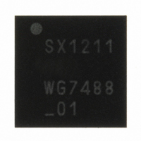
SX1211I084TRT Semtech, SX1211I084TRT Datasheet - Page 59

SX1211I084TRT
Manufacturer Part Number
SX1211I084TRT
Description
IC SNGL-CHIP TXRX 32-TQFN
Manufacturer
Semtech
Specifications of SX1211I084TRT
Frequency
860 ~ 960MHz
Data Rate - Maximum
200kbps
Modulation Or Protocol
FSK, OOK
Applications
AMR, ISM, Security and Access
Power - Output
12.5dBm
Sensitivity
-113dBm
Voltage - Supply
2.1 V ~ 3.6 V
Current - Receiving
3mA
Current - Transmitting
25mA
Data Interface
PCB, Surface Mount
Antenna Connector
PCB, Surface Mount
Operating Temperature
-40°C ~ 85°C
Package / Case
32-TQFN
Operating Temperature (min)
-40C
Operating Temperature (max)
85C
Operating Temperature Classification
Industrial
Modulation Type
FSK/OOK
Package Type
TQFN EP
Operating Supply Voltage (min)
2.1V
Operating Supply Voltage (typ)
2.5/3.3V
Operating Supply Voltage (max)
3.6V
Lead Free Status / RoHS Status
Lead free / RoHS Compliant
Memory Size
-
Lead Free Status / Rohs Status
Compliant
Other names
SX1211I084TRT
Available stocks
Company
Part Number
Manufacturer
Quantity
Price
Company:
Part Number:
SX1211I084TRT
Manufacturer:
HITTITE
Quantity:
560
Rev 7 – Sept 2
ADVANCED COMMUNICATIONS & SENSING
Data_mode_1
IF_gain
Freq_dev
Res
BR
OOK_
floor_thresh
Fifo_size
Fifo_thresh
R1
P1
S1
R2
P2
S2
Res
PA_ramp
Res
nd
, 2008
2
1-0
7-0
7
6-0
7-0
7:6
5-0
7-0
7-0
7-0
7-0
7-0
7-0
7-5
4-3
2-0
1
1
2
3
3
4
5
5
6
7
8
9
10
11
12
12
12
r/w
r/w
r/w
r/w
r/w
r/w
r/w
r/w
r/w
r/w
r/w
r/w
r/w
r/w
r/w
r/w
r/w
Data operation mode’s MSB. Cf. Data_mode_0 (Bit 5 Addr 1)
Gain on the IF chain:
00
01
10
11
Single side frequency deviation in FSK Transmit mode:
Refer to sections 3.3.4 and 3.3.5
Fdev =
(d): D = “00000011” => Fdev = 100 kHz
Reserved
(d): “0”
Bit Rate =
(d): C = “0000111” => Bit Rate = 25 kb/s NRZ
Floor threshold in OOK Rx mode. By default 6 dB.
(d): “00001100” assuming 0.5 dB RSSI step
FIFO size selection:
00
01
10
11
FIFO threshold for interrupt source (Cf section 5.2.2.3)
(d): B = “001111”
R counter, active when RPS_select=”0”
(d):77h; default values of R1, P1, S1 generate 915.0 MHz in FSK mode
P counter, active when RPS_select=”0”
(d): 64h; default values of R1, P1, S1 generate 915.0 MHz in FSK mode
S counter, active when RPS_select=”0”
(d): 32h; default values of R1, P1, S1 generate 915.0 MHz in FSK mode
R counter, active when RPS_select=”1”
(d): 74h; default values of R2, P2, S2 generate 920.0 MHz in FSK mode
P counter, active when RPS_select=”1”
(d): 62h; default values of R2, P2, S2 generate 920.0 MHz in FSK mode
S counter, active when RPS_select=”1”
(d): 32h; default values of R2, P2, S2 generate 920.0 MHz in FSK mode
Reserved
(d): “001”
Ramp control of the rise and fall times of the Tx PA regulator output voltage in
OOK mode:
00
01
10
11
Reserved
(d):”000”
Data_mode_1
Bit 2 addr 1
maximal gain (0dB) (d)
-4.5 dB
-9dB
-13.5 dB
16 bytes (d)
32 bytes
48 bytes
64 bytes
3us
8.5 us
15 us
23 us (d)
32
0
0
1
Page 59 of 92
64
f
(D
XTAL
f
XTAL
(C
1)
Data_mode_0
Bit 5 addr 1
, 0 ≤ D ≤ 255, where D is the value in the register.
1)
, 0 ≤ C ≤ 127, where C is the value in the register.
0
1
x
Data Operation
Mode
Continuous (d)
Buffered
Packet
www.semtech.com
SX1211


