DSP56F803BU80 Freescale Semiconductor, DSP56F803BU80 Datasheet - Page 46
DSP56F803BU80
Manufacturer Part Number
DSP56F803BU80
Description
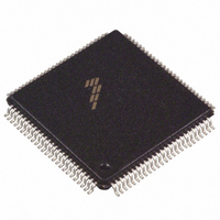
IC DSP 80MHZ 31.5K FLASH 100LQFP
Manufacturer
Freescale Semiconductor
Series
56F8xxr
Datasheet
1.DSP56F803BU80E.pdf
(52 pages)
Specifications of DSP56F803BU80
Core Processor
56800
Core Size
16-Bit
Speed
80MHz
Connectivity
CAN, EBI/EMI, SCI, SPI
Peripherals
POR, PWM, WDT
Number Of I /o
16
Program Memory Size
71KB (35.5K x 16)
Program Memory Type
FLASH
Ram Size
2.5K x 16
Voltage - Supply (vcc/vdd)
3 V ~ 3.6 V
Data Converters
A/D 8x12b
Oscillator Type
External
Operating Temperature
-40°C ~ 85°C
Package / Case
100-LQFP
Lead Free Status / RoHS Status
Contains lead / RoHS non-compliant
Eeprom Size
-
Available stocks
Company
Part Number
Manufacturer
Quantity
Price
Company:

Part Number:
DSP56F803BU80
Manufacturer:
MOTOLOLA
Quantity:
996
Company:
Part Number:
DSP56F803BU80
Manufacturer:
Freescale Semiconductor
Quantity:
10 000
Part Number:
DSP56F803BU80
Manufacturer:
FREESCALE
Quantity:
20 000
Company:
Part Number:
DSP56F803BU803
Manufacturer:
FREESCAL
Quantity:
329
Company:
Part Number:
DSP56F803BU80E
Manufacturer:
SHARP
Quantity:
5 600
Company:
Part Number:
DSP56F803BU80E
Manufacturer:
FREESCAL
Quantity:
364
Company:
Part Number:
DSP56F803BU80E
Manufacturer:
Freescale Semiconductor
Quantity:
10 000
Part Number:
DSP56F803BU80E
Manufacturer:
FREESCALE
Quantity:
20 000


3.14 JTAG Timing
46
TCK frequency of operation
TCK cycle time
TCK clock pulse width
TMS, TDI data set-up time
TMS, TDI data hold time
TCK low to TDO data valid
TCK low to TDO tri-state
TRST assertion time
DE assertion time
Operating Conditions:
1. Timing is both wait state and frequency dependent. For the values listed, T = clock cycle. For 80MHz
operation, T = 12.5ns.
2. TCK frequency of operation must be less than 1/8 the processor rate.
3. Parameters listed are guaranteed by design.
(Input)
TCK
V
M
= V
IL
+ (V
Characteristic
IH
Figure 3-28 Test Clock Input Timing Diagram
– V
2
V
IL
SS
)/2
V
= V
IH
SSA
Table 3-18 JTAG Timing
= 0 V, V
56F803 Technical Data, Rev. 16
DD
t
PW
= V
V
V
M
IL
DDA
= 3.0–3.6 V, T
Symbol
t
t
CY
TRST
t
f
t
t
t
t
t
t
PW
OP
DH
CY
DS
DV
TS
DE
A
1, 3
= –40° to +85°C, C
t
PW
Min
100
DC
0.4
1.2
V
50
50
4T
—
—
M
L
Max
26.6
23.5
≤
10
—
—
—
—
—
—
Freescale Semiconductor
50pF, f
OP
= 80MHz
MHz
Unit
ns
ns
ns
ns
ns
ns
ns
ns
Related parts for DSP56F803BU80
Image
Part Number
Description
Manufacturer
Datasheet
Request
R

Part Number:
Description:
Manufacturer:
Freescale Semiconductor, Inc
Datasheet:
Part Number:
Description:
Manufacturer:
Freescale Semiconductor, Inc
Datasheet:
Part Number:
Description:
Manufacturer:
Freescale Semiconductor, Inc
Datasheet:
Part Number:
Description:
Manufacturer:
Freescale Semiconductor, Inc
Datasheet:
Part Number:
Description:
Manufacturer:
Freescale Semiconductor, Inc
Datasheet:
Part Number:
Description:
Manufacturer:
Freescale Semiconductor, Inc
Datasheet:
Part Number:
Description:
Manufacturer:
Freescale Semiconductor, Inc
Datasheet:
Part Number:
Description:
Manufacturer:
Freescale Semiconductor, Inc
Datasheet:
Part Number:
Description:
Manufacturer:
Freescale Semiconductor, Inc
Datasheet:
Part Number:
Description:
Manufacturer:
Freescale Semiconductor, Inc
Datasheet:
Part Number:
Description:
Manufacturer:
Freescale Semiconductor, Inc
Datasheet:
Part Number:
Description:
Manufacturer:
Freescale Semiconductor, Inc
Datasheet:
Part Number:
Description:
Manufacturer:
Freescale Semiconductor, Inc
Datasheet:
Part Number:
Description:
Manufacturer:
Freescale Semiconductor, Inc
Datasheet:
Part Number:
Description:
Manufacturer:
Freescale Semiconductor, Inc
Datasheet: