DSP56F803BU80 Freescale Semiconductor, DSP56F803BU80 Datasheet - Page 12
DSP56F803BU80
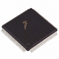
Manufacturer Part Number
DSP56F803BU80
Description
IC DSP 80MHZ 31.5K FLASH 100LQFP
Manufacturer
Freescale Semiconductor
Series
56F8xxr
Datasheet
1.DSP56F803BU80E.pdf
(52 pages)
Specifications of DSP56F803BU80
Core Processor
56800
Core Size
16-Bit
Speed
80MHz
Connectivity
CAN, EBI/EMI, SCI, SPI
Peripherals
POR, PWM, WDT
Number Of I /o
16
Program Memory Size
71KB (35.5K x 16)
Program Memory Type
FLASH
Ram Size
2.5K x 16
Voltage - Supply (vcc/vdd)
3 V ~ 3.6 V
Data Converters
A/D 8x12b
Oscillator Type
External
Operating Temperature
-40°C ~ 85°C
Package / Case
100-LQFP
Lead Free Status / RoHS Status
Contains lead / RoHS non-compliant
Eeprom Size
-
Available stocks
Company
Part Number
Manufacturer
Quantity
Price
Company:

Part Number:
DSP56F803BU80
Manufacturer:
MOTOLOLA
Quantity:
996
Company:
Part Number:
DSP56F803BU80
Manufacturer:
Freescale Semiconductor
Quantity:
10 000
Part Number:
DSP56F803BU80
Manufacturer:
FREESCALE
Quantity:
20 000
Company:
Part Number:
DSP56F803BU803
Manufacturer:
FREESCAL
Quantity:
329
Company:
Part Number:
DSP56F803BU80E
Manufacturer:
SHARP
Quantity:
5 600
Company:
Part Number:
DSP56F803BU80E
Manufacturer:
FREESCAL
Quantity:
364
Company:
Part Number:
DSP56F803BU80E
Manufacturer:
Freescale Semiconductor
Quantity:
10 000
Part Number:
DSP56F803BU80E
Manufacturer:
FREESCALE
Quantity:
20 000


2.5 Interrupt and Program Control Signals
12
No. of
No. of
No. of
Pins
Pins
Pins
1
1
1
1
16
1
1
Signal
Name
WR
DS
RD
PS
D0–D15
Signal
Name
Signal
IRQA
IRQB
Name
Signal
Output
Output
Output
Output
Type
Input/O
Signal
(Schmitt)
(Schmitt)
Type
utput
Signal
Table 2-9 Interrupt and Program Control Signals
Type
Input
Input
State During
Tri-stated
Tri-stated
Tri-stated
Tri-stated
Reset
State During
Tri-stated
State During
Table 2-8 Bus Control Signals
Reset
Reset
Table 2-7 Data Bus Signals
Input
Input
56F803 Technical Data, Rev. 16
Program Memory Select—PS is asserted low for external Program memory
access.
Data Memory Select—DS is asserted low for external Data memory access.
Write Enable—WR is asserted during external memory write cycles. When
WR is asserted low, pins D0–D15 become outputs and the device puts data
on the bus. When WR is deasserted high, the external data is latched inside
the external device. When WR is asserted, it qualifies the A0–A15, PS, and
DS pins. WR can be connected directly to the WE pin of a Static RAM.
Read Enable—RD is asserted during external memory read cycles. When
RD is asserted low, pins D0–D15 become inputs and an external device is
enabled onto the device data bus. When RD is deasserted high, the external
data is latched inside the controller. When RD is asserted, it qualifies the
A0–A15, PS, and DS pins. RD can be connected directly to the OE pin of a
Static RAM or ROM.
Data Bus— D0–D15 specify the data for external Program or Data
memory accesses. D0–D15 are tri-stated when the external bus is
inactive. Internal pull-ups may be active.
External Interrupt Request A—The IRQA input is a synchronized
external interrupt request indicating an external device is requesting
service. It can be programmed to be level-sensitive or
negative-edge- triggered.
External Interrupt Request B—The IRQB input is an external
interrupt request indicating an external device is requesting service.
It can be programmed to be level-sensitive or
negative-edge-triggered.
Signal Description
Signal Description
Signal Description
Freescale Semiconductor
Related parts for DSP56F803BU80
Image
Part Number
Description
Manufacturer
Datasheet
Request
R

Part Number:
Description:
Manufacturer:
Freescale Semiconductor, Inc
Datasheet:
Part Number:
Description:
Manufacturer:
Freescale Semiconductor, Inc
Datasheet:
Part Number:
Description:
Manufacturer:
Freescale Semiconductor, Inc
Datasheet:
Part Number:
Description:
Manufacturer:
Freescale Semiconductor, Inc
Datasheet:
Part Number:
Description:
Manufacturer:
Freescale Semiconductor, Inc
Datasheet:
Part Number:
Description:
Manufacturer:
Freescale Semiconductor, Inc
Datasheet:
Part Number:
Description:
Manufacturer:
Freescale Semiconductor, Inc
Datasheet:
Part Number:
Description:
Manufacturer:
Freescale Semiconductor, Inc
Datasheet:
Part Number:
Description:
Manufacturer:
Freescale Semiconductor, Inc
Datasheet:
Part Number:
Description:
Manufacturer:
Freescale Semiconductor, Inc
Datasheet:
Part Number:
Description:
Manufacturer:
Freescale Semiconductor, Inc
Datasheet:
Part Number:
Description:
Manufacturer:
Freescale Semiconductor, Inc
Datasheet:
Part Number:
Description:
Manufacturer:
Freescale Semiconductor, Inc
Datasheet:
Part Number:
Description:
Manufacturer:
Freescale Semiconductor, Inc
Datasheet:
Part Number:
Description:
Manufacturer:
Freescale Semiconductor, Inc
Datasheet: