DSP56F803BU80 Freescale Semiconductor, DSP56F803BU80 Datasheet - Page 17
DSP56F803BU80
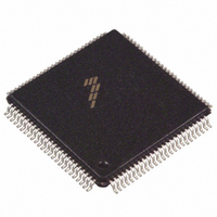
Manufacturer Part Number
DSP56F803BU80
Description
IC DSP 80MHZ 31.5K FLASH 100LQFP
Manufacturer
Freescale Semiconductor
Series
56F8xxr
Datasheet
1.DSP56F803BU80E.pdf
(52 pages)
Specifications of DSP56F803BU80
Core Processor
56800
Core Size
16-Bit
Speed
80MHz
Connectivity
CAN, EBI/EMI, SCI, SPI
Peripherals
POR, PWM, WDT
Number Of I /o
16
Program Memory Size
71KB (35.5K x 16)
Program Memory Type
FLASH
Ram Size
2.5K x 16
Voltage - Supply (vcc/vdd)
3 V ~ 3.6 V
Data Converters
A/D 8x12b
Oscillator Type
External
Operating Temperature
-40°C ~ 85°C
Package / Case
100-LQFP
Lead Free Status / RoHS Status
Contains lead / RoHS non-compliant
Eeprom Size
-
Available stocks
Company
Part Number
Manufacturer
Quantity
Price
Company:

Part Number:
DSP56F803BU80
Manufacturer:
MOTOLOLA
Quantity:
996
Company:
Part Number:
DSP56F803BU80
Manufacturer:
Freescale Semiconductor
Quantity:
10 000
Part Number:
DSP56F803BU80
Manufacturer:
FREESCALE
Quantity:
20 000
Company:
Part Number:
DSP56F803BU803
Manufacturer:
FREESCAL
Quantity:
329
Company:
Part Number:
DSP56F803BU80E
Manufacturer:
SHARP
Quantity:
5 600
Company:
Part Number:
DSP56F803BU80E
Manufacturer:
FREESCAL
Quantity:
364
Company:
Part Number:
DSP56F803BU80E
Manufacturer:
Freescale Semiconductor
Quantity:
10 000
Part Number:
DSP56F803BU80E
Manufacturer:
FREESCALE
Quantity:
20 000


2.13 JTAG/OnCE
Part 3 Specifications
3.1 General Characteristics
The 56F803 is fabricated in high-density CMOS with 5-V tolerant TTL-compatible digital inputs. The
term “5-V tolerant” refers to the capability of an I/O pin, built on a 3.3V-compatible process technology,
to withstand a voltage up to 5.5V without damaging the device. Many systems have a mixture of devices
designed for 3.3V and 5V power supplies. In such systems, a bus may carry both 3.3V and 5V-compatible
I/O voltage levels (a standard 3.3V I/O is designed to receive a maximum voltage of 3.3V ± 10% during
normal operation without causing damage). This 5V-tolerant capability therefore offers the power savings
of 3.3V I/O levels while being able to receive 5V levels without being damaged.
Freescale Semiconductor
No. of
Pins
1
1
1
1
1
1
Signal
Name
TRST
TCK
TMS
TDO
TDI
DE
(Schmitt)
(Schmitt)
(Schmitt)
(Schmitt)
Signal
Output
Output
Type
Input
Input
Input
Input
Table 2-17 JTAG/On-Chip Emulation (OnCE) Signals
Input, pulled low
high internally
high internally
high internally
State During
Input, pulled
Input, pulled
Input, pulled
Tri-stated
internally
Output
Reset
56F803 Technical Data, Rev. 16
Test Clock Input—This input pin provides a gated clock to synchronize the
test logic and shift serial data to the JTAG/OnCE port. The pin is connected
internally to a pull-down resistor.
Test Mode Select Input—This input pin is used to sequence the JTAG
TAP controller’s state machine. It is sampled on the rising edge of TCK and
has an on-chip pull-up resistor.
Note:
Test Data Input—This input pin provides a serial input data stream to the
JTAG/OnCE port. It is sampled on the rising edge of TCK and has an
on-chip pull-up resistor.
Test Data Output—This tri-statable output pin provides a serial output data
stream from the JTAG/OnCE port. It is driven in the Shift-IR and Shift-DR
controller states, and changes on the falling edge of TCK.
Test Reset—As an input, a low signal on this pin provides a reset signal to
the JTAG TAP controller. To ensure complete hardware reset, TRST
should be asserted at power-up and whenever RESET is asserted. The
only exception occurs in a debugging environment when a hardware device
reset is required and it is necessary not to reset the OnCE/JTAG module. In
this case, assert RESET, but do not assert TRST.
Note:
used in a debugging environment, TRST may be tied to V
Debug Event—DE provides a low pulse on recognized debug events.
Always tie the TMS pin to V
For normal operation, connect TRST directly to V
Signal Description
DD
through a 2.2K resistor.
SS
SS
through a 1K resistor.
. If the design is to be
JTAG/OnCE
17
Related parts for DSP56F803BU80
Image
Part Number
Description
Manufacturer
Datasheet
Request
R

Part Number:
Description:
Manufacturer:
Freescale Semiconductor, Inc
Datasheet:
Part Number:
Description:
Manufacturer:
Freescale Semiconductor, Inc
Datasheet:
Part Number:
Description:
Manufacturer:
Freescale Semiconductor, Inc
Datasheet:
Part Number:
Description:
Manufacturer:
Freescale Semiconductor, Inc
Datasheet:
Part Number:
Description:
Manufacturer:
Freescale Semiconductor, Inc
Datasheet:
Part Number:
Description:
Manufacturer:
Freescale Semiconductor, Inc
Datasheet:
Part Number:
Description:
Manufacturer:
Freescale Semiconductor, Inc
Datasheet:
Part Number:
Description:
Manufacturer:
Freescale Semiconductor, Inc
Datasheet:
Part Number:
Description:
Manufacturer:
Freescale Semiconductor, Inc
Datasheet:
Part Number:
Description:
Manufacturer:
Freescale Semiconductor, Inc
Datasheet:
Part Number:
Description:
Manufacturer:
Freescale Semiconductor, Inc
Datasheet:
Part Number:
Description:
Manufacturer:
Freescale Semiconductor, Inc
Datasheet:
Part Number:
Description:
Manufacturer:
Freescale Semiconductor, Inc
Datasheet:
Part Number:
Description:
Manufacturer:
Freescale Semiconductor, Inc
Datasheet:
Part Number:
Description:
Manufacturer:
Freescale Semiconductor, Inc
Datasheet: