DSP56F803BU80 Freescale Semiconductor, DSP56F803BU80 Datasheet - Page 44
DSP56F803BU80
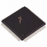
Manufacturer Part Number
DSP56F803BU80
Description
IC DSP 80MHZ 31.5K FLASH 100LQFP
Manufacturer
Freescale Semiconductor
Series
56F8xxr
Datasheet
1.DSP56F803BU80E.pdf
(52 pages)
Specifications of DSP56F803BU80
Core Processor
56800
Core Size
16-Bit
Speed
80MHz
Connectivity
CAN, EBI/EMI, SCI, SPI
Peripherals
POR, PWM, WDT
Number Of I /o
16
Program Memory Size
71KB (35.5K x 16)
Program Memory Type
FLASH
Ram Size
2.5K x 16
Voltage - Supply (vcc/vdd)
3 V ~ 3.6 V
Data Converters
A/D 8x12b
Oscillator Type
External
Operating Temperature
-40°C ~ 85°C
Package / Case
100-LQFP
Lead Free Status / RoHS Status
Contains lead / RoHS non-compliant
Eeprom Size
-
Available stocks
Company
Part Number
Manufacturer
Quantity
Price
Company:

Part Number:
DSP56F803BU80
Manufacturer:
MOTOLOLA
Quantity:
996
Company:
Part Number:
DSP56F803BU80
Manufacturer:
Freescale Semiconductor
Quantity:
10 000
Part Number:
DSP56F803BU80
Manufacturer:
FREESCALE
Quantity:
20 000
Company:
Part Number:
DSP56F803BU803
Manufacturer:
FREESCAL
Quantity:
329
Company:
Part Number:
DSP56F803BU80E
Manufacturer:
SHARP
Quantity:
5 600
Company:
Part Number:
DSP56F803BU80E
Manufacturer:
FREESCAL
Quantity:
364
Company:
Part Number:
DSP56F803BU80E
Manufacturer:
Freescale Semiconductor
Quantity:
10 000
Part Number:
DSP56F803BU80E
Manufacturer:
FREESCALE
Quantity:
20 000


3.13 Controller Area Network (CAN) Timing
44
1. Parasitic capacitance due to package, pin to pin, and pin to package base coupling. (1.8pf)
2. Parasitic capacitance due to the chip bond pad, ESD protection devices and signal routing. (2.04pf)
3. Equivalent resistance for the ESD isolation resistor and the channel select mux. (500 ohms)
4. Sampling capacitor at the sample and hold circuit. (1pf)
Operating Conditions: V
Baud Rate
Bus Wakeup detection
ADC Quiescent Current (both ADCs)
V
1. For optimum ADC performance, keep the minimum V
output code of 0.
2. V
DA
3. Measured in 10-90% range.
4. LSB = Least Significant Bit.
5. Guaranteed by characterization.
6. t
REF
-0.3V.
AIC
Quiescent Current (both ADCs)
REF
= 1/
must be equal to or less than V
ADC analog input
f
Characteristic
ADIC
Characteristic
SS
1
= V
Figure 3-26 Equivalent Analog Input Circuit
SSA
1
= 0 V, V
Table 3-16 ADC Characteristics
DDA
DD
Table 3-17 CAN Timing
56F803 Technical Data, Rev. 16
and must be greater than 2.7V. For optimal ADC performance, set V
= V
Symbol
DDA
T
I
2
Symbol
I
VREF
BR
ADC
WAKEUP
= 3.0–3.6 V, T
CAN
ADCIN
value > 25mV. Inputs less than 25mV may convert to a digital
Min
—
—
A
= –40× to +85×C, C
Min
—
5
3
2
Typ
50
12
L
£ 50pF, MSCAN Clock = 30MHz
4
Max
Max
16.5
—
—
1
Freescale Semiconductor
REF
Unit
to V
Mbps
mA
mA
Unit
μs
D-
Related parts for DSP56F803BU80
Image
Part Number
Description
Manufacturer
Datasheet
Request
R

Part Number:
Description:
Manufacturer:
Freescale Semiconductor, Inc
Datasheet:
Part Number:
Description:
Manufacturer:
Freescale Semiconductor, Inc
Datasheet:
Part Number:
Description:
Manufacturer:
Freescale Semiconductor, Inc
Datasheet:
Part Number:
Description:
Manufacturer:
Freescale Semiconductor, Inc
Datasheet:
Part Number:
Description:
Manufacturer:
Freescale Semiconductor, Inc
Datasheet:
Part Number:
Description:
Manufacturer:
Freescale Semiconductor, Inc
Datasheet:
Part Number:
Description:
Manufacturer:
Freescale Semiconductor, Inc
Datasheet:
Part Number:
Description:
Manufacturer:
Freescale Semiconductor, Inc
Datasheet:
Part Number:
Description:
Manufacturer:
Freescale Semiconductor, Inc
Datasheet:
Part Number:
Description:
Manufacturer:
Freescale Semiconductor, Inc
Datasheet:
Part Number:
Description:
Manufacturer:
Freescale Semiconductor, Inc
Datasheet:
Part Number:
Description:
Manufacturer:
Freescale Semiconductor, Inc
Datasheet:
Part Number:
Description:
Manufacturer:
Freescale Semiconductor, Inc
Datasheet:
Part Number:
Description:
Manufacturer:
Freescale Semiconductor, Inc
Datasheet:
Part Number:
Description:
Manufacturer:
Freescale Semiconductor, Inc
Datasheet: