DSP56F803BU80 Freescale Semiconductor, DSP56F803BU80 Datasheet
DSP56F803BU80
Specifications of DSP56F803BU80
Available stocks


Related parts for DSP56F803BU80

DSP56F803BU80 Summary of contents
Page 1
Data Sheet Preliminary Technical Data 56F800 16-bit Digital Signal Controllers DSP56F803 Rev. 16 09/2007 freescale.com ...
Page 2
Version History Rev. 16 Added revision history. Added this text to footnote any particular percent of the low pulse width.” Document Revision History Description of Change Table 3-8: “However, the high pulse width does not have to ...
Page 3
... Applica- tion-Specific SPI or Memory & GPIO 4 Peripherals * includes TCS pin which is reserved for factory use and is tied to VSS Freescale Semiconductor • 6-channel PWM module • Two 4-channel 12-bit ADCs • Quadrature Decoder • CAN 2.0 B module • Serial Communication Interface (SCI) • ...
Page 4
... Freescale’s patented dead time distortion correction • Two 12 bit Analog-to-Digital Converters (ADCs), which support two simultaneous conversions; ADC and - PWM modules can be synchronized • Quadrature Decoder with four inputs (shares pins with Quad Timer) 4 56F803 Technical Data, Rev. 16 Freescale Semiconductor ...
Page 5
... JTAG port) with 512 words of Program RAM and 2K words of Data RAM. It also supports program execution from external memory. A total of 2K words of Boot Flash is incorporated for easy customer-inclusion of field-programmable Freescale Semiconductor tolerant, TTL-compatible digital inputs - 56F803 Technical Data, Rev. 16 ...
Page 6
... A complete set of evaluation modules (EVMs) and development system cards will support concurrent engineering. Together, PE, Code Warrior and EVMs create a complete, scalable tools solution for easy, fast, and efficient development. 6 erased or erased in page sizes of 256 words. – erased. - 56F803 Technical Data, Rev. 16 Freescale Semiconductor ...
Page 7
... Product Documentation The four documents listed in Table 1-1 56F803. Documentation is available from local Freescale distributors, Freescale Semiconductor sales offices, Freescale Literature Distribution Centers, or online at: www.freescale.com Table 1-1 56F803 Chip Documentation Topic 56800E Detailed description of the 56800 family architecture, and Family Manual ...
Page 8
... Technical Data, Rev. 16 Detailed Pins Description 7 Table 2-2 7 Table 2-3 2 Table 2-4 3 Table 2-5 16 Table 2-6 16 Table 2-7 4 Table 2-8 4 Table 2-9 12 Table 2-10 4 Table 2-11 4 Table 2-12 2 Table 2-13 2 Table 2-14 9 Table 2-15 2 Table 2-16 6 Table 2-17 Freescale Semiconductor Table 2-1 ...
Page 9
... Quadrature PHASEB0 (TA1) Decoder or Quad Timer A INDEX0 (TA2) HOME0 (TA3) JTAG/OnCE™ Port * includes TCS pin which is reserved for factory use and is tied to VSS Figure 2-1 56F803 Signals Identified by Functional Group 1. Alternate pin functionality is shown in parenthesis. Freescale Semiconductor DDA 1 V SSA ...
Page 10
... VCAPC—Connect each pin to a 2.2 μF or greater bypass capacitor in Supply order to bypass the core logic voltage regulator (required for proper chip operation). For more information, please refer to 56F803 Technical Data, Rev. 16 for normal use. SS SS. Signal Description Section 5.2. Freescale Semiconductor ...
Page 11
... A8–A15 Output GPIOA0 Input/O – GPIOA7 utput Freescale Semiconductor Table 2-5 PLL and Clock Reset Input External Crystal Oscillator Input—This input should be connected to an 8MHz external crystal or ceramic resonator. For more information, please refer to Section Crystal Oscillator Output—This output should be connected to an 8MHz external crystal or ceramic resonator ...
Page 12
... It can be programmed to be level-sensitive or negative-edge- triggered. Input External Interrupt Request B—The IRQB input is an external interrupt request indicating an external device is requesting service. It can be programmed to be level-sensitive or negative-edge-triggered. 56F803 Technical Data, Rev. 16 Signal Description Signal Description Signal Description Freescale Semiconductor ...
Page 13
... Input FAULTA0 2 (Schmitt) Freescale Semiconductor State During Reset Input Reset—This input is a direct hardware reset on the processor. When RESET is asserted low, the controller is initialized and placed in the Reset state. A Schmitt trigger input is used for noise immunity. When the RESET pin is deasserted, the initial chip operating mode is latched from the EXTBOOT pin ...
Page 14
... SPI Slave Select—In master mode, this pin is used to arbitrate multiple masters. In slave mode, this pin is used to select the slave. Port E GPIO—This General Purpose I/O (GPIO) pin can be Input individually programmed as an input or output pin. After reset, the default state is SS. 56F803 Technical Data, Rev. 16 Signal Description Freescale Semiconductor ...
Page 15
... Pins Name 1 TXD0 Output GPIOE0 Input/Output 1 RXD0 Input GPIOE1 Input/Output Freescale Semiconductor State During Reset Input Phase A—Quadrature Decoder #0 PHASEA input Input TA0—Timer A Channel 0 Input Phase B—Quadrature Decoder #0 PHASEB input Input TA1—Timer A Channel 1 Input Index—Quadrature Decoder #0 INDEX input Input TA2— ...
Page 16
... Input VREF—Analog reference voltage for ADC. Must be set to V for optimal performance. Signal Type State During Reset Input/Output Input 56F803 Technical Data, Rev. 16 Signal Description Signal Description DDA Signal Description – – TD1 2— Timer D Channel 1 2 Freescale Semiconductor -0.3V ...
Page 17
... I/O voltage levels (a standard 3.3V I/O is designed to receive a maximum voltage of 3.3V ± 10% during normal operation without causing damage). This 5V-tolerant capability therefore offers the power savings of 3.3V I/O levels while being able to receive 5V levels without being damaged. Freescale Semiconductor Reset Test Clock Input—This input pin provides a gated clock to synchronize the test logic and shift serial data to the JTAG/OnCE port ...
Page 18
... PWM outputs, TCS Symbol Min V 3 3.0 DDA ΔV -0.1 DD 56F803 Technical Data, Rev. 16 Min Max V – – 0.3 0 0.3 0 – 0 0.3 IN SSA DDA V – 0 3.0 IN SSA SSA I — 10 Typ Max 3.3 3.6 3.3 3.6 - 0.1 Freescale Semiconductor Unit Unit ...
Page 19
... The basic cold plate measurement technique is described by MIL-STD 883D, Method 1012.1. This is the correct thermal metric to use to calculate thermal performance when the package is being used with a heat sink. Freescale Semiconductor Symbol Min Δ ...
Page 20
... Typ Max Unit 2.25 — 2.75 0 — 0.5 2.2 — 5.5 -0.3 — 0.8 2.0 — 5.5 -0.3 — 0.8 μA -1 — 1 μA -1 — 1 μA -1 — 1 μA -210 — -50 μA 20 — 180 μA -1 — KΩ μA -10 — 10 μA -10 — 10 Freescale Semiconductor ...
Page 21
... All inputs 0.2V from rail; outputs unloaded. All ports configured DD as inputs; measured with all modules enabled. 7. Wait I measured using external square wave clock source (f DD loads; less than 50pF on all outputs. C wait I ; measured with PLL enabled. DD Freescale Semiconductor = 3.0–3 SSA DD DDA Symbol 2 ...
Page 22
... IDD Total 20 40 Freq. (MHz) are tested using the V and and V for an input signal are shown 56F803 Technical Data, Rev generally connected to the same potential and the point when the V interrupt is DD EIO 60 Table 3-14) levels specified in the DC Characteristics Freescale Semiconductor 80 ...
Page 23
... Mode XE Standby L Read H Word Program H Page Erase H Mass Erase address enable, all rows are disabled when address enable, YMUX is disabled when Sense amplifier enable 4. Output enable, tri-state Flash data out bus when Freescale Semiconductor Low – Data2 Valid Data2 Tri-stated Figure 3-3 Signal States ...
Page 24
... Figure – us Figure 3-4 – ms Figure 3-5 – ms Figure 3-6 – cycles – years – us Figure 3-4, Figure 3-5, Figure 3-6 – us Figure 3-4, Figure 3-5 – us Figure 3-6 – us Figure 3-4 – us Figure 3-4, Figure 3-5, Figure 3-6 Freescale Semiconductor ...
Page 25
... Parameters are guaranteed by design in smart programming mode and must be one cycle or greater. *The Flash interface unit provides registers for the control of these parameters. IFREN XADR XE YADR YE DIN PROG Tnvs NVSTR Freescale Semiconductor 3.0–3.6V SSA DD DDA Symbol Min ...
Page 26
... IFREN XADR XE YE=SE=OE=MAS1=0 ERASE Tnvs NVSTR IFREN XADR XE MAS1 YE=SE=OE=0 ERASE Tnvs NVSTR 26 Terase Figure 3-5 Flash Erase Cycle Tme Figure 3-6 Flash Mass Erase Cycle 56F803 Technical Data, Rev. 16 Tnvh Trcv Tnvh1 Trcv Freescale Semiconductor ...
Page 27
... CL1 * CL2 CL = CL1 + CL2 This is the value load capacitance that should be used when selecting a crystal and determining the actual frequency of operation of the crystal oscillator circuit. EXTAL XTAL Figure 3-7 Connecting to a Crystal Oscillator Freescale Semiconductor Table 3- 9pF Recommended External Crystal ...
Page 28
... Figure 3-9 Connecting an External Clock Signal 28 Figure 3-8, a typical ceramic resonator circuit is no external load capacitors should be used. Recommended Ceramic Resonator Parameters MΩ 8MHz (optimized for 8MHz 56F803 XTAL EXTAL V External SS Clock 56F803 Technical Data, Rev. 16 Figure 3-9. The external clock Freescale Semiconductor ...
Page 29
... The high or low pulse width must be no smaller than 6.25ns or the chip will not function. However, the high pulse width does not have to be any particular percent of the low pulse width. 3. Parameters listed are guaranteed by design. External 90% 50% Clock 10 Note: The midpoint Freescale Semiconductor SSA DD DDA Symbol Min 1 f ...
Page 30
... OCCS chapter in the out 1, 2 ≤ = 80MHz = –40° to +85°C, C 50pF Min Max 6.5 — 7.5 — — — 4.2 4.8 — 2.2 — — 0 — — 18.7 Freescale Semiconductor Unit MHz MHz ms ms Unit ...
Page 31
... Address Valid to Input Data Valid Wait states = 0 Wait states > 0 Address Valid to RD Asserted RD Asserted to Input Data Valid Wait states = 0 Wait states > Deasserted to RD Asserted RD Deasserted to RD Asserted WR Deasserted to WR Asserted RD Deasserted to WR Asserted Freescale Semiconductor = 3.0–3 SSA DD DDA Symbol t DRD ...
Page 32
... Min t — RAZ 275,000T 128T t 33T RDA 56F803 Technical Data, Rev ARDD t RDA t RDRD RDWR t RDD t DRD Data ≤ = –40° to +85°C, C 50pF A L Max Unit See Figure 21 ns Figure 3-12 Figure 3-12 — ns — ns 34T ns Figure 3-12 Freescale Semiconductor ...
Page 33
... The minimum is specified for the duration of an edge-sensitive IRQA interrupt required to recover from the Stop state. This is not the minimum required so that the IRQA interrupt is accepted. 4. The interrupt instruction fetch is visible on the pins only in Mode 3. 5. Parameters listed are guaranteed by design. Freescale Semiconductor 3.0– ...
Page 34
... RESET t RAZ A0–A15, D0–D15 PS, DS, RD, WR Figure 3-12 Asynchronous Reset Timing IRQA, IRQB Figure 3-13 External Interrupt Timing (Negative-Edge-Sensitive IRW 56F803 Technical Data, Rev RDA First Fetch First Fetch Freescale Semiconductor ...
Page 35
... Figure 3-15 Interrupt from Wait State Timing t IW IRQA A0–A15, PS, DS, RD, WR Figure 3-16 Recovery from Stop State Using Asynchronous Interrupt Timing Freescale Semiconductor Reset, Stop, Wait, Mode Select, and Interrupt Timing First Interrupt Instruction Execution a) First Interrupt Instruction Execution b) General Purpose I/O t IRI t IF 56F803 Technical Data, Rev ...
Page 36
... Figure — — ns — Figures 3-18, , — ns 3-20, — Figures 3-18, , — ns 3-20, 25 — ns Figures 3-18 — ns 3-20, 0 — ns Figures 3-18 — ns 3-20, 2 — ns Figure 15 ns Figure 15.2 ns Freescale Semiconductor 3-21 3-21 3-21 3-21 3-21 3-21 3-21 3-21 3-21 ...
Page 37
... Rise time Master Slave Fall time Master Slave 1. Parameters listed are guaranteed by design. SS (Input) SCLK (CPOL = 0) (Output) SCLK (CPOL = 1) (Output) MISO (Input) MOSI (Output) Figure 3-18 SPI Master Timing (CPHA = 0) Freescale Semiconductor Table 3-12 SPI Timing = 3.0–3.6V, T SSA DD DDA Symbol ...
Page 38
... SS (Input) SCLK (CPOL = 0) (Output) SCLK (CPOL = 1) (Output) MISO (Input) (ref MOSI (Output) Figure 3-19 SPI Master Timing (CPHA = held High on master MSB in Bits 14– Master MSB out Bits 14– 56F803 Technical Data, Rev LSB Master LSB out t R Freescale Semiconductor ...
Page 39
... SS (Input) SCLK (CPOL = 0) (Input) SCLK (CPOL = 1) (Input) MISO (Output MOSI (Input) Figure 3-20 SPI Slave Timing (CPHA = 0) Freescale Semiconductor ELD Slave MSB out Bits 14– MSB in Bits 14–1 56F803 Technical Data, Rev. 16 Serial Peripheral Interface (SPI) Timing ELG Slave LSB out ...
Page 40
... MSB in Bits 14–1 Table 3-13 Timer Timing = 3.0–3.6V, T SSA DD DDA Symbol Min P 4T 2T+3 INHL P 2T OUT 56F803 Technical Data, Rev ELG Slave LSB out LSB ≤ = –40° to +85°C, C 50pF 80MHz Max Unit — ns — ns — ns Freescale Semiconductor ...
Page 41
... Quadrature input period Quadrature input high/low period Quadrature phase period 1. In the formulas listed clock cycle. For 80MHz operation 12. ns. V ≤ –40° to +85° Parameters listed are guaranteed by design. Freescale Semiconductor Table 3-13 Timer Timing = 3.0–3.6V, T SSA DD DDA P 1T ...
Page 42
... Table 3-15 SCI Timing = 3.0–3 SSA DD DDA Symbol Min BR — RXD 0.965/BR PW TXD 0.965/BR PW RXD PW Figure 3-24 RXD Pulse Width 56F803 Technical Data, Rev ≤ = –40° to +85°C, C 50pF 80MHz Max Unit (f *2.5)/(80) Mbps MAX 1.04/BR ns 1.04/BR ns Freescale Semiconductor ...
Page 43
... Sample time Input capacitance 5 Gain Error (transfer gain) 5 Offset Voltage 5 Total Harmonic Distortion 5 Signal-to-Noise plus Distortion 5 Effective Number of Bits 5 Spurious Free Dynamic Range Bandwidth Freescale Semiconductor TXD PW Figure 3-25 TXD Pulse Width Table 3-16 ADC Characteristics Symbol Min ADCIN INL — ...
Page 44
... For optimal ADC performance, set V DDA 3 2 Table 3-17 CAN Timing = V = 3.0–3 –40× to +85× DDA A Symbol Min BR — CAN T 5 WAKEUP 56F803 Technical Data, Rev. 16 Typ Max Unit 50 — 16 REF £ 50pF, MSCAN Clock = 30MHz L Max Unit 1 Mbps μs — Freescale Semiconductor ...
Page 45
... CAN wakeup message consists of 5 dominant bits at the highest possible baud rate of 1Mbps. 2. Parameters listed are guaranteed by design. MSCAN_RX CAN receive data pin (Input) Freescale Semiconductor T WAKEUP Figure 3-27 Bus Wakeup Detection 56F803 Technical Data, Rev. 16 Controller Area Network (CAN) Timing ...
Page 46
... Figure 3-28 Test Clock Input Timing Diagram 46 Table 3-18 JTAG Timing = 3.0–3 SSA DD DDA Symbol TRST )/2 56F803 Technical Data, Rev ≤ = –40° to +85°C, C 50pF 80MHz Min Max Unit DC 10 MHz 100 — — ns 0.4 — ns 1.2 — ns — 26.6 ns — 23 — — Freescale Semiconductor ...
Page 47
... TCK (Input) TDI TMS (Input) TDO (Output) TDO (Output ) TDO (Output) Figure 3-29 Test Access Port Timing Diagram TRST (Input Freescale Semiconductor t DS Input Data Valid TRST Figure 3-30 TRST Timing Diagram DE Figure 3-31 OnCE—Debug Event 56F803 Technical Data, Rev ...
Page 48
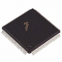
... A13 V DD PIN Figure 4-1 Top View, 56F803 100-pin LQFP Package 48 ORIENTATION MARK 56F803 Technical Data, Rev. 16 PWMA5 PIN 76 PWMA4 PWMA3 PWMA2 PWMA1 PWMA0 HOME0 INDEX0 PHASEB0 PHASEA0 DDA V SSA EXTAL XTAL AN7 AN6 AN5 PIN 51 AN4 AN3 AN2 Freescale Semiconductor ...
Page 49
... D10 2 D11 3 D12 4 D13 5 D14 6 D15 A10 20 A11 21 A12 22 A13 Freescale Semiconductor Signal Name Pin No. 26 A14 51 27 A15 IRQA 56 32 IRQB 57 33 TCS 58 34 TCK 59 35 TMS 60 36 TDI 61 37 TDO 62 38 TRST 63 39 VCAPC 64 40 ISA0 65 41 ISA1 66 42 ...
Page 50
... K 0.500 0.700 0.020 0.028 ° ° REF 12 REF N 0.090 0.160 0.004 0.006 ° ° ° 0.150 0.250 0.006 0.010 S 15.950 16.050 0.628 0.632 V 15.950 16.050 0.628 0.632 W 0.200 REF 0.008 REF X 1.000 REF 0.039 REF Freescale Semiconductor ° ...
Page 51
... Measure the thermal resistance from the junction to the outside surface of the package (case) closest to the chip mounting area when that surface has a proper heat sink. This is done to minimize temperature variation Freescale Semiconductor , in °C can be obtained from the equation: J × ...
Page 52
... Freescale Semiconductor was negligent regarding the design or manufacture of the part. Freescale™ and the Freescale logo are trademarks of Freescale Semiconductor, Inc. All other product or service names are the property of their respective owners. This product incorporates SuperFlash® ...