DSP56F803BU80 Freescale Semiconductor, DSP56F803BU80 Datasheet - Page 30
DSP56F803BU80
Manufacturer Part Number
DSP56F803BU80
Description
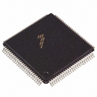
IC DSP 80MHZ 31.5K FLASH 100LQFP
Manufacturer
Freescale Semiconductor
Series
56F8xxr
Datasheet
1.DSP56F803BU80E.pdf
(52 pages)
Specifications of DSP56F803BU80
Core Processor
56800
Core Size
16-Bit
Speed
80MHz
Connectivity
CAN, EBI/EMI, SCI, SPI
Peripherals
POR, PWM, WDT
Number Of I /o
16
Program Memory Size
71KB (35.5K x 16)
Program Memory Type
FLASH
Ram Size
2.5K x 16
Voltage - Supply (vcc/vdd)
3 V ~ 3.6 V
Data Converters
A/D 8x12b
Oscillator Type
External
Operating Temperature
-40°C ~ 85°C
Package / Case
100-LQFP
Lead Free Status / RoHS Status
Contains lead / RoHS non-compliant
Eeprom Size
-
Available stocks
Company
Part Number
Manufacturer
Quantity
Price
Company:

Part Number:
DSP56F803BU80
Manufacturer:
MOTOLOLA
Quantity:
996
Company:
Part Number:
DSP56F803BU80
Manufacturer:
Freescale Semiconductor
Quantity:
10 000
Part Number:
DSP56F803BU80
Manufacturer:
FREESCALE
Quantity:
20 000
Company:
Part Number:
DSP56F803BU803
Manufacturer:
FREESCAL
Quantity:
329
Company:
Part Number:
DSP56F803BU80E
Manufacturer:
SHARP
Quantity:
5 600
Company:
Part Number:
DSP56F803BU80E
Manufacturer:
FREESCAL
Quantity:
364
Company:
Part Number:
DSP56F803BU80E
Manufacturer:
Freescale Semiconductor
Quantity:
10 000
Part Number:
DSP56F803BU80E
Manufacturer:
FREESCALE
Quantity:
20 000


3.5.4
3.6 External Bus Asynchronous Timing
30
Operating Conditions:
External reference crystal frequency for the PLL
PLL output frequency
PLL stabilization time
PLL stabilization time
Address Valid to WR Asserted
WR Width Asserted
Wait states = 0
Wait states > 0
WR Asserted to D0–D15 Out Valid
Data Out Hold Time from WR Deasserted
Data Out Set Up Time to WR Deasserted
Wait states = 0
Wait states > 0
RD Deasserted to Address Not Valid
Address Valid to RD Deasserted
Wait states = 0
Wait states > 0
1. An externally supplied reference clock should be as free as possible from any phase jitter for the PLL to work
correctly. The PLL is optimized for 8MHz input crystal.
2. ZCLK may not exceed 80MHz. For additional information on ZCLK and f
User Manual. ZCLK = f
3. This is the minimum time required after the PLL set-up is changed to ensure reliable operation.
Phase Locked Loop Timing
Operating Conditions:
Characteristic
Characteristic
3
Table 3-10 External Bus Asynchronous Timing
op
3
2
-40
0
o
o
to +85
V
to 0
SS
= V
o
C
o
C
SSA
= 0 V, V
V
56F803 Technical Data, Rev. 16
Table 3-9 PLL Timing
SS
= V
DD
1
SSA
= V
= 0 V, V
DDA
Symbol
t
t
t
Symbol
t
t
t
ARDD
AWR
t
WRD
DOH
DOS
RDA
WR
f
= 3.0–3.6 V, T
out
f
t
t
osc
plls
plls
DD
/2
= V
DDA
(T*WS) + 18.7
(T*WS) + 7.5
(T*WS) + 6.4
out
Min
40
A
= 3.0–3.6 V, T
—
—
4
/2, please refer to the OCCS chapter in the
= –40° to +85°C, C
18.7
Min
6.5
7.5
4.8
2.2
—
0
Typ
100
—
8
1
A
= –40° to +85°C
1, 2
L
≤
Max
50pF, f
4.2
—
—
—
—
—
—
—
—
Freescale Semiconductor
Max
110
200
10
10
op
= 80MHz
MHz
MHz
Unit
ms
ms
Unit
ns
ns
ns
ns
ns
ns
ns
ns
ns
ns
Related parts for DSP56F803BU80
Image
Part Number
Description
Manufacturer
Datasheet
Request
R

Part Number:
Description:
Manufacturer:
Freescale Semiconductor, Inc
Datasheet:
Part Number:
Description:
Manufacturer:
Freescale Semiconductor, Inc
Datasheet:
Part Number:
Description:
Manufacturer:
Freescale Semiconductor, Inc
Datasheet:
Part Number:
Description:
Manufacturer:
Freescale Semiconductor, Inc
Datasheet:
Part Number:
Description:
Manufacturer:
Freescale Semiconductor, Inc
Datasheet:
Part Number:
Description:
Manufacturer:
Freescale Semiconductor, Inc
Datasheet:
Part Number:
Description:
Manufacturer:
Freescale Semiconductor, Inc
Datasheet:
Part Number:
Description:
Manufacturer:
Freescale Semiconductor, Inc
Datasheet:
Part Number:
Description:
Manufacturer:
Freescale Semiconductor, Inc
Datasheet:
Part Number:
Description:
Manufacturer:
Freescale Semiconductor, Inc
Datasheet:
Part Number:
Description:
Manufacturer:
Freescale Semiconductor, Inc
Datasheet:
Part Number:
Description:
Manufacturer:
Freescale Semiconductor, Inc
Datasheet:
Part Number:
Description:
Manufacturer:
Freescale Semiconductor, Inc
Datasheet:
Part Number:
Description:
Manufacturer:
Freescale Semiconductor, Inc
Datasheet:
Part Number:
Description:
Manufacturer:
Freescale Semiconductor, Inc
Datasheet: