DSP56F803BU80 Freescale Semiconductor, DSP56F803BU80 Datasheet - Page 11
DSP56F803BU80
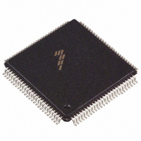
Manufacturer Part Number
DSP56F803BU80
Description
IC DSP 80MHZ 31.5K FLASH 100LQFP
Manufacturer
Freescale Semiconductor
Series
56F8xxr
Datasheet
1.DSP56F803BU80E.pdf
(52 pages)
Specifications of DSP56F803BU80
Core Processor
56800
Core Size
16-Bit
Speed
80MHz
Connectivity
CAN, EBI/EMI, SCI, SPI
Peripherals
POR, PWM, WDT
Number Of I /o
16
Program Memory Size
71KB (35.5K x 16)
Program Memory Type
FLASH
Ram Size
2.5K x 16
Voltage - Supply (vcc/vdd)
3 V ~ 3.6 V
Data Converters
A/D 8x12b
Oscillator Type
External
Operating Temperature
-40°C ~ 85°C
Package / Case
100-LQFP
Lead Free Status / RoHS Status
Contains lead / RoHS non-compliant
Eeprom Size
-
Available stocks
Company
Part Number
Manufacturer
Quantity
Price
Company:

Part Number:
DSP56F803BU80
Manufacturer:
MOTOLOLA
Quantity:
996
Company:
Part Number:
DSP56F803BU80
Manufacturer:
Freescale Semiconductor
Quantity:
10 000
Part Number:
DSP56F803BU80
Manufacturer:
FREESCALE
Quantity:
20 000
Company:
Part Number:
DSP56F803BU803
Manufacturer:
FREESCAL
Quantity:
329
Company:
Part Number:
DSP56F803BU80E
Manufacturer:
SHARP
Quantity:
5 600
Company:
Part Number:
DSP56F803BU80E
Manufacturer:
FREESCAL
Quantity:
364
Company:
Part Number:
DSP56F803BU80E
Manufacturer:
Freescale Semiconductor
Quantity:
10 000
Part Number:
DSP56F803BU80E
Manufacturer:
FREESCALE
Quantity:
20 000


2.3 Clock and Phase Locked Loop Signals
2.4 Address, Data, and Bus Control Signals
Freescale Semiconductor
No. of
No. of
Pins
Pins
1
1
1
6
2
8
GPIOE2
GPIOA0
GPIOE3
GPIOA7
A8–A15
EXTAL
A0–A5
A6–A7
Signal
Signal
CLKO
Name
Name
XTAL
–
–
Input/O
Input/O
Signal
Output
Output
Output
Signal
Output
Output
Type
utput
utput
Input/
Type
Input
State During
State During
Chip-driven
Chip-driven
Tri-stated
Tri-stated
Tri-stated
Reset
Input
Input
Reset
Input
Table 2-6 Address Bus Signals
Table 2-5 PLL and Clock
56F803 Technical Data, Rev. 16
Address Bus—A0–A5 specify the address for external Program or Data
memory accesses.
Address Bus—A6–A7 specify the address for external Program or Data
memory accesses.
Port E GPIO—These two pins are General Purpose I/O (GPIO) pins that
can be individually programmed as input or output pins.
After reset, the default state is Address Bus.
Address Bus—A8–A15 specify the address for external Program or
Data memory accesses.
Port A GPIO—These eight pins are General Purpose I/O (GPIO) pins
that can be individually programmed as input or output pins.
After reset, the default state is Address Bus.
External Crystal Oscillator Input—This input should be connected to
an 8MHz external crystal or ceramic resonator. For more information,
please refer to
Crystal Oscillator Output—This output should be connected to an
8MHz external crystal or ceramic resonator. For more information,
please refer to
This pin can also be connected to an external clock source. For more
information, please refer to
Clock Output—This pin outputs a buffered clock signal. By
programming the CLKOSEL[4:0] bits in the CLKO Select Register
(CLKOSR), the user can select between outputting a version of the
signal applied to XTAL and a version of the device’s master clock at the
output of the PLL. The clock frequency on this pin can also be disabled
by programming the CLKOSEL[4:0] bits in CLKOSR.
Section
Section
3.5.
3.5.
Signal Description
Signal Description
Section
3.5.3.
Clock and Phase Locked Loop Signals
11
Related parts for DSP56F803BU80
Image
Part Number
Description
Manufacturer
Datasheet
Request
R

Part Number:
Description:
Manufacturer:
Freescale Semiconductor, Inc
Datasheet:
Part Number:
Description:
Manufacturer:
Freescale Semiconductor, Inc
Datasheet:
Part Number:
Description:
Manufacturer:
Freescale Semiconductor, Inc
Datasheet:
Part Number:
Description:
Manufacturer:
Freescale Semiconductor, Inc
Datasheet:
Part Number:
Description:
Manufacturer:
Freescale Semiconductor, Inc
Datasheet:
Part Number:
Description:
Manufacturer:
Freescale Semiconductor, Inc
Datasheet:
Part Number:
Description:
Manufacturer:
Freescale Semiconductor, Inc
Datasheet:
Part Number:
Description:
Manufacturer:
Freescale Semiconductor, Inc
Datasheet:
Part Number:
Description:
Manufacturer:
Freescale Semiconductor, Inc
Datasheet:
Part Number:
Description:
Manufacturer:
Freescale Semiconductor, Inc
Datasheet:
Part Number:
Description:
Manufacturer:
Freescale Semiconductor, Inc
Datasheet:
Part Number:
Description:
Manufacturer:
Freescale Semiconductor, Inc
Datasheet:
Part Number:
Description:
Manufacturer:
Freescale Semiconductor, Inc
Datasheet:
Part Number:
Description:
Manufacturer:
Freescale Semiconductor, Inc
Datasheet:
Part Number:
Description:
Manufacturer:
Freescale Semiconductor, Inc
Datasheet: