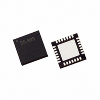
C8051F351-GMR Silicon Laboratories Inc, C8051F351-GMR Datasheet - Page 68

C8051F351-GMR
Manufacturer Part Number
C8051F351-GMR
Description
IC 8051 MCU 8K FLASH 28MLP
Manufacturer
Silicon Laboratories Inc
Series
C8051F35xr
Specifications of C8051F351-GMR
Core Processor
8051
Core Size
8-Bit
Speed
50MHz
Connectivity
SMBus (2-Wire/I²C), SPI, UART/USART
Peripherals
POR, PWM, Temp Sensor, WDT
Number Of I /o
17
Program Memory Size
8KB (8K x 8)
Program Memory Type
FLASH
Ram Size
768 x 8
Voltage - Supply (vcc/vdd)
2.7 V ~ 3.6 V
Data Converters
A/D 8x24b; D/A 2x8b
Oscillator Type
Internal
Operating Temperature
-40°C ~ 85°C
Package / Case
28-VQFN Exposed Pad, 28-HVQFN, 28-SQFN, 28-DHVQFN
Processor Series
C8051F3x
Core
8051
Data Bus Width
8 bit
Data Ram Size
768 B
Interface Type
I2C, SMBus, SPI, UART
Maximum Clock Frequency
50 MHz
Number Of Programmable I/os
17
Number Of Timers
4
Maximum Operating Temperature
+ 85 C
Mounting Style
SMD/SMT
3rd Party Development Tools
KSK-SL-TOOLSTICK, PK51, CA51, A51, ULINK2
Development Tools By Supplier
C8051F350DK
Minimum Operating Temperature
- 40 C
On-chip Adc
24 bit, 8 Channel
On-chip Dac
8 bit, 2 Channel
For Use With
336-1083 - DEV KIT FOR F350/351/352/353
Lead Free Status / RoHS Status
Lead free / RoHS Compliant
Eeprom Size
-
Lead Free Status / Rohs Status
Details
- Current page: 68 of 234
- Download datasheet (2Mb)
C8051F350/1/2/3
6.1.
A flexible output update mechanism allows for seamless full-scale changes and supports jitter-free
updates for waveform generation. Three update modes are provided, allowing IDAC output updates on a
write to the IDAC’s data register, on a Timer overflow, or on an external pin edge.
6.1.1. Update Output On-Demand
In its default mode (IDAnCN.[6:4] = ‘111’) the IDAC output is updated “on-demand” with a write to the data
register (IDAn). In this mode, data is immediately latched into the IDAC after a write to its data register.
6.1.2. Update Output Based on Timer Overflow
The IDAC output update can be scheduled on a Timer overflow. This feature is useful in systems where the
IDAC is used to generate a waveform of a defined sampling rate, by eliminating the effects of variable
interrupt latency and instruction execution on the timing of the IDAC output. When the IDAnCM bits
(IDAnCN.[6:4]) are set to ‘000’, ‘001’, ‘010’ or ‘011’, writes to the IDAC data register (IDAn) are held until an
associated Timer overflow event (Timer 0, Timer 1, Timer 2 or Timer 3, respectively) occurs, at which time
the data register contents are copied to the IDAC input latch, allowing the IDAC output to change to the
new value.
6.1.3. Update Output Based on CNVSTR Edge
The IDAC output can also be configured to update on a rising edge, falling edge, or both edges of the
external CNVSTR signal. When the IDAnCM bits (IDAnCN.[6:4]) are set to ‘100’, ‘101’, or ‘110’, writes to
the IDAC data register (IDAn) are held until an edge occurs on the CNVSTR input pin. The particular set-
ting of the IDAnCM bits determines whether the IDAC output is updated on rising, falling, or both edges of
CNVSTR. When a corresponding edge occurs, the data register contents are copied to the IDAC input
latch, allowing the IDAC output to change to the new value.
6.2.
The data word mapping for the IDAC is shown in Figure 6.2. The full-scale output current of the IDAC is
selected using the IDAnOMD bits (IDAnCN[1:0]). By default, the IDAC is set to a full-scale output current of
0.25 mA. The IDAnOMD bits can also be configured to provide full-scale output currents of 0.5 mA, 1 mA,
or 2 mA.
68
IDAn Data Word
(D7 – D0)
IDAC Output Scheduling
IDAC Output Mapping
0xFF
0x00
0x01
0x80
128/256 x 2 mA
255/256 x 2 mA
1/256 x 2 mA
‘11’ (2 mA)
Figure 6.2. IDAC Data Word Mapping
0 mA
Output Current vs IDAnOMD bit setting
128/256 x 1 mA
255/256 x 1 mA
1/256 x 1 mA
‘10’ (1 mA)
Rev. 1.1
0 mA
128/256 x 0.5 mA 128/256 x 0.25 mA
255/256 x 0.5 mA 255/256 x 0.25 mA
1/256 x 0.5 mA
‘01’ (0.5 mA)
0 mA
1/256 x 0.25 mA
‘00’ (0.25 mA)
0 mA
Related parts for C8051F351-GMR
Image
Part Number
Description
Manufacturer
Datasheet
Request
R
Part Number:
Description:
SMD/C°/SINGLE-ENDED OUTPUT SILICON OSCILLATOR
Manufacturer:
Silicon Laboratories Inc
Part Number:
Description:
Manufacturer:
Silicon Laboratories Inc
Datasheet:
Part Number:
Description:
N/A N/A/SI4010 AES KEYFOB DEMO WITH LCD RX
Manufacturer:
Silicon Laboratories Inc
Datasheet:
Part Number:
Description:
N/A N/A/SI4010 SIMPLIFIED KEY FOB DEMO WITH LED RX
Manufacturer:
Silicon Laboratories Inc
Datasheet:
Part Number:
Description:
N/A/-40 TO 85 OC/EZLINK MODULE; F930/4432 HIGH BAND (REV E/B1)
Manufacturer:
Silicon Laboratories Inc
Part Number:
Description:
EZLink Module; F930/4432 Low Band (rev e/B1)
Manufacturer:
Silicon Laboratories Inc
Part Number:
Description:
I°/4460 10 DBM RADIO TEST CARD 434 MHZ
Manufacturer:
Silicon Laboratories Inc
Part Number:
Description:
I°/4461 14 DBM RADIO TEST CARD 868 MHZ
Manufacturer:
Silicon Laboratories Inc
Part Number:
Description:
I°/4463 20 DBM RFSWITCH RADIO TEST CARD 460 MHZ
Manufacturer:
Silicon Laboratories Inc
Part Number:
Description:
I°/4463 20 DBM RADIO TEST CARD 868 MHZ
Manufacturer:
Silicon Laboratories Inc
Part Number:
Description:
I°/4463 27 DBM RADIO TEST CARD 868 MHZ
Manufacturer:
Silicon Laboratories Inc
Part Number:
Description:
I°/4463 SKYWORKS 30 DBM RADIO TEST CARD 915 MHZ
Manufacturer:
Silicon Laboratories Inc
Part Number:
Description:
N/A N/A/-40 TO 85 OC/4463 RFMD 30 DBM RADIO TEST CARD 915 MHZ
Manufacturer:
Silicon Laboratories Inc
Part Number:
Description:
I°/4463 20 DBM RADIO TEST CARD 169 MHZ
Manufacturer:
Silicon Laboratories Inc


