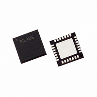
C8051F351-GMR Silicon Laboratories Inc, C8051F351-GMR Datasheet - Page 47

C8051F351-GMR
Manufacturer Part Number
C8051F351-GMR
Description
IC 8051 MCU 8K FLASH 28MLP
Manufacturer
Silicon Laboratories Inc
Series
C8051F35xr
Specifications of C8051F351-GMR
Core Processor
8051
Core Size
8-Bit
Speed
50MHz
Connectivity
SMBus (2-Wire/I²C), SPI, UART/USART
Peripherals
POR, PWM, Temp Sensor, WDT
Number Of I /o
17
Program Memory Size
8KB (8K x 8)
Program Memory Type
FLASH
Ram Size
768 x 8
Voltage - Supply (vcc/vdd)
2.7 V ~ 3.6 V
Data Converters
A/D 8x24b; D/A 2x8b
Oscillator Type
Internal
Operating Temperature
-40°C ~ 85°C
Package / Case
28-VQFN Exposed Pad, 28-HVQFN, 28-SQFN, 28-DHVQFN
Processor Series
C8051F3x
Core
8051
Data Bus Width
8 bit
Data Ram Size
768 B
Interface Type
I2C, SMBus, SPI, UART
Maximum Clock Frequency
50 MHz
Number Of Programmable I/os
17
Number Of Timers
4
Maximum Operating Temperature
+ 85 C
Mounting Style
SMD/SMT
3rd Party Development Tools
KSK-SL-TOOLSTICK, PK51, CA51, A51, ULINK2
Development Tools By Supplier
C8051F350DK
Minimum Operating Temperature
- 40 C
On-chip Adc
24 bit, 8 Channel
On-chip Dac
8 bit, 2 Channel
For Use With
336-1083 - DEV KIT FOR F350/351/352/353
Lead Free Status / RoHS Status
Lead free / RoHS Compliant
Eeprom Size
-
Lead Free Status / Rohs Status
Details
- Current page: 47 of 234
- Download datasheet (2Mb)
5.3.1. Error Conditions
Any errors during a conversion or calibration are indicated using bits in the ADC0STA register. The
AD0S3C flag will be set to ‘1’ if there is a SINC3 filter clip during the conversion. Likewise, the AD0FFC
flag will be set to ‘1’ if there is a Fast filter clip during the conversion. A filter clip occurs whenever an inter-
nal filter register overflows during a conversion. The AD0OVR flag will be set to ‘1’ if an ADC overrun con-
dition occurs. An overrun occurs if the end of a conversion is reached while the AD0INT flag is still set to ‘1’
from the previous conversion. If the data registers have not been read, the new data values will be
updated, and the previous conversion will be lost. The general AD0ERR flag indicates that an AD0S3C,
AD0FFC, or AD0OVR error condition has occurred, or that a calibration resulted in a value that was
beyond the limits of the offset or gain register. The data output registers are updated at the end of every
conversion regardless of whether or not an error occurs.
5.4.
An 8-bit offset DAC is included, which can be used for offset correction up to approximately ±1/2 of the
ADC’s input range on any PGA gain setting. The ADC0DAC register (SFR Definition 5.7) controls the off-
set DAC voltage. The register is decoded as a signed binary word. The MSB (bit 7) determines the sign of
the DAC magnitude (0 = positive, 1 = negative), and the remaining seven bits (bits 6–0) determine the
magnitude. Each LSB of the offset DAC is equivalent to approximately 0.4% of the ADC’s input span. A
write to the ADC0DAC register initiates a change on the offset DAC output.
5.5.
The burnout current sources can be used to detect an open circuit or short circuit at the ADC inputs. The
burnout current sources are enabled by setting the AD0BCE bit in register ADC0CN to ‘1’ (SFR Definition
5.1). The positive-channel burnout current source sources approximately 2 µA on AIN+, and the negative-
channel burnout current sinks approximately 2 µA on AIN–. If an open circuit exists between AIN+ and
AIN– when the burnout current sources are enabled, the ADC will read a full scale positive value. If a
short-circuit exists between AIN+ and AIN– when the burnout current sources are enabled, the ADC will
read a value near zero. The burnout current sources should be disabled during normal ADC measure-
ments.
*Note: Input Voltage is voltage at ADC inputs after amplification by the PGA.
Input Voltage* (AIN+ – AIN–) 24-bit Output Word (C8051F350/1) 16-bit Output Word (C8051F352/3)
*Note: Input Voltage is voltage at ADC inputs after amplification by the PGA.
Input Voltage* (AIN+ – AIN–) 24-bit Output Word (C8051F350/1) 16-bit Output Word (C8051F352/3)
VREF – 1 LSB
VREF – 1 LSB
Offset DAC
Burnout Current Sources
–VREF / 2
VREF / 2
VREF / 2
+1 LSB
+1 LSB
–1 LSB
–VREF
Table 5.1. ADC0 Unipolar Output Word Coding (AD0POL = 0)
0
Table 5.2. ADC0 Bipolar Output Word Coding (AD0POL = 1)
0
0xFFFFFF
0x800000
0x000001
0x000000
0xFFFFFF
0x7FFFFF
0xC00000
0x400000
0x000001
0x000000
0x800000
Rev. 1.1
C8051F350/1/2/3
0xFFFF
0x8000
0x0001
0x0000
0x7FFF
0xFFFF
0xC000
0x4000
0x0001
0x0000
0x8000
47
Related parts for C8051F351-GMR
Image
Part Number
Description
Manufacturer
Datasheet
Request
R
Part Number:
Description:
SMD/C°/SINGLE-ENDED OUTPUT SILICON OSCILLATOR
Manufacturer:
Silicon Laboratories Inc
Part Number:
Description:
Manufacturer:
Silicon Laboratories Inc
Datasheet:
Part Number:
Description:
N/A N/A/SI4010 AES KEYFOB DEMO WITH LCD RX
Manufacturer:
Silicon Laboratories Inc
Datasheet:
Part Number:
Description:
N/A N/A/SI4010 SIMPLIFIED KEY FOB DEMO WITH LED RX
Manufacturer:
Silicon Laboratories Inc
Datasheet:
Part Number:
Description:
N/A/-40 TO 85 OC/EZLINK MODULE; F930/4432 HIGH BAND (REV E/B1)
Manufacturer:
Silicon Laboratories Inc
Part Number:
Description:
EZLink Module; F930/4432 Low Band (rev e/B1)
Manufacturer:
Silicon Laboratories Inc
Part Number:
Description:
I°/4460 10 DBM RADIO TEST CARD 434 MHZ
Manufacturer:
Silicon Laboratories Inc
Part Number:
Description:
I°/4461 14 DBM RADIO TEST CARD 868 MHZ
Manufacturer:
Silicon Laboratories Inc
Part Number:
Description:
I°/4463 20 DBM RFSWITCH RADIO TEST CARD 460 MHZ
Manufacturer:
Silicon Laboratories Inc
Part Number:
Description:
I°/4463 20 DBM RADIO TEST CARD 868 MHZ
Manufacturer:
Silicon Laboratories Inc
Part Number:
Description:
I°/4463 27 DBM RADIO TEST CARD 868 MHZ
Manufacturer:
Silicon Laboratories Inc
Part Number:
Description:
I°/4463 SKYWORKS 30 DBM RADIO TEST CARD 915 MHZ
Manufacturer:
Silicon Laboratories Inc
Part Number:
Description:
N/A N/A/-40 TO 85 OC/4463 RFMD 30 DBM RADIO TEST CARD 915 MHZ
Manufacturer:
Silicon Laboratories Inc
Part Number:
Description:
I°/4463 20 DBM RADIO TEST CARD 169 MHZ
Manufacturer:
Silicon Laboratories Inc


