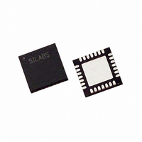
C8051F351-GMR Silicon Laboratories Inc, C8051F351-GMR Datasheet - Page 106

C8051F351-GMR
Manufacturer Part Number
C8051F351-GMR
Description
IC 8051 MCU 8K FLASH 28MLP
Manufacturer
Silicon Laboratories Inc
Series
C8051F35xr
Specifications of C8051F351-GMR
Core Processor
8051
Core Size
8-Bit
Speed
50MHz
Connectivity
SMBus (2-Wire/I²C), SPI, UART/USART
Peripherals
POR, PWM, Temp Sensor, WDT
Number Of I /o
17
Program Memory Size
8KB (8K x 8)
Program Memory Type
FLASH
Ram Size
768 x 8
Voltage - Supply (vcc/vdd)
2.7 V ~ 3.6 V
Data Converters
A/D 8x24b; D/A 2x8b
Oscillator Type
Internal
Operating Temperature
-40°C ~ 85°C
Package / Case
28-VQFN Exposed Pad, 28-HVQFN, 28-SQFN, 28-DHVQFN
Processor Series
C8051F3x
Core
8051
Data Bus Width
8 bit
Data Ram Size
768 B
Interface Type
I2C, SMBus, SPI, UART
Maximum Clock Frequency
50 MHz
Number Of Programmable I/os
17
Number Of Timers
4
Maximum Operating Temperature
+ 85 C
Mounting Style
SMD/SMT
3rd Party Development Tools
KSK-SL-TOOLSTICK, PK51, CA51, A51, ULINK2
Development Tools By Supplier
C8051F350DK
Minimum Operating Temperature
- 40 C
On-chip Adc
24 bit, 8 Channel
On-chip Dac
8 bit, 2 Channel
For Use With
336-1083 - DEV KIT FOR F350/351/352/353
Lead Free Status / RoHS Status
Lead free / RoHS Compliant
Eeprom Size
-
Lead Free Status / Rohs Status
Details
- Current page: 106 of 234
- Download datasheet (2Mb)
C8051F350/1/2/3
is made to service the pending interrupt. Therefore, the maximum response time for an interrupt (when no
other interrupt is currently being serviced or the new interrupt is of greater priority) occurs when the CPU is
performing an RETI instruction followed by a DIV as the next instruction. In this case, the response time is
18 system clock cycles: 1 clock cycle to detect the interrupt, 5 clock cycles to execute the RETI, 8 clock
cycles to complete the DIV instruction and 4 clock cycles to execute the LCALL to the ISR. If the CPU is
executing an ISR for an interrupt with equal or higher priority, the new interrupt will not be serviced until the
current ISR completes, including the RETI and following instruction.
106
Interrupt Source
Reset
External Interrupt 0
(/INT0)
Timer 0 Overflow
External Interrupt 1
(/INT1)
Timer 1 Overflow
UART0
Timer 2 Overflow
SPI0
SMB0
RESERVED
RESERVED
ADC0
Programmable Counter
Array
Comparator0
RESERVED
Timer 3 Overflow
Interrupt
0x000B
0x001B
0x002B
0x003B
0x004B
0x005B
0x006B
0x0000
0x0003
0x0013
0x0023
0x0033
0x0043
0x0053
0x0063
0x0073
Vector
Table 12.1. Interrupt Summary
Priority
Order
Top
10
11
12
13
14
0
1
2
3
4
5
6
7
8
9
AD0INT (ADC0STA.5)
RXOVRN (SPI0CN.4)
CP0RIF (CPT0CN.5)
CP0FIF (CPT0CN.4)
Rev. 1.1
TF2H (TMR2CN.7)
CCFn (PCA0CN.n)
TF3H (TMR3CN.7)
WCOL (SPI0CN.6)
MODF (SPI0CN.5)
TF2L (TMR2CN.6)
TF3L (TMR3CN.6)
SPIF (SPI0CN.7)
CF (PCA0CN.7)
SI (SMB0CN.0)
RI0 (SCON0.0)
TI0 (SCON0.1)
Pending Flag
TF0 (TCON.5)
TF1 (TCON.7)
IE0 (TCON.1)
IE1 (TCON.3)
None
N/A
N/A
N/A
N/A N/A
N/A N/A
N/A N/A
N/A N/A
Y
Y
Y
Y
Y
Y
Y
Y
Y
Y
N
N
Y
Y
Y
Y
N
N
N
N
N
N
N
N
EX0 (IE.0) PX0 (IP.0)
ET0 (IE.1) PT0 (IP.1)
EX1 (IE.2) PX1 (IP.2)
ET1 (IE.3) PT1 (IP.3)
ES0 (IE.4) PS0 (IP.4)
ET2 (IE.5) PT2 (IP.5)
(EIE1.0)
(EIE1.3)
(EIE1.4)
Enabled
(EIE1.5)
(EIE1.7)
ESMB0
EADC0
Enable
EPCA0
Always
ESPI0
ECP0
(IE.6)
Flag
ET3
N/A
N/A
N/A
(EIP1.0)
(EIP1.3)
(EIP1.4)
(EIP1.5)
(EIP1.7)
Priority
Control
Highest
PSMB0
PADC0
PPCA0
Always
PSPI0
PCP0
(IP.6)
PT3
N/A
N/A
N/A
Related parts for C8051F351-GMR
Image
Part Number
Description
Manufacturer
Datasheet
Request
R
Part Number:
Description:
SMD/C°/SINGLE-ENDED OUTPUT SILICON OSCILLATOR
Manufacturer:
Silicon Laboratories Inc
Part Number:
Description:
Manufacturer:
Silicon Laboratories Inc
Datasheet:
Part Number:
Description:
N/A N/A/SI4010 AES KEYFOB DEMO WITH LCD RX
Manufacturer:
Silicon Laboratories Inc
Datasheet:
Part Number:
Description:
N/A N/A/SI4010 SIMPLIFIED KEY FOB DEMO WITH LED RX
Manufacturer:
Silicon Laboratories Inc
Datasheet:
Part Number:
Description:
N/A/-40 TO 85 OC/EZLINK MODULE; F930/4432 HIGH BAND (REV E/B1)
Manufacturer:
Silicon Laboratories Inc
Part Number:
Description:
EZLink Module; F930/4432 Low Band (rev e/B1)
Manufacturer:
Silicon Laboratories Inc
Part Number:
Description:
I°/4460 10 DBM RADIO TEST CARD 434 MHZ
Manufacturer:
Silicon Laboratories Inc
Part Number:
Description:
I°/4461 14 DBM RADIO TEST CARD 868 MHZ
Manufacturer:
Silicon Laboratories Inc
Part Number:
Description:
I°/4463 20 DBM RFSWITCH RADIO TEST CARD 460 MHZ
Manufacturer:
Silicon Laboratories Inc
Part Number:
Description:
I°/4463 20 DBM RADIO TEST CARD 868 MHZ
Manufacturer:
Silicon Laboratories Inc
Part Number:
Description:
I°/4463 27 DBM RADIO TEST CARD 868 MHZ
Manufacturer:
Silicon Laboratories Inc
Part Number:
Description:
I°/4463 SKYWORKS 30 DBM RADIO TEST CARD 915 MHZ
Manufacturer:
Silicon Laboratories Inc
Part Number:
Description:
N/A N/A/-40 TO 85 OC/4463 RFMD 30 DBM RADIO TEST CARD 915 MHZ
Manufacturer:
Silicon Laboratories Inc
Part Number:
Description:
I°/4463 20 DBM RADIO TEST CARD 169 MHZ
Manufacturer:
Silicon Laboratories Inc


