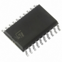
ST72F623F2M1 STMicroelectronics, ST72F623F2M1 Datasheet - Page 88

ST72F623F2M1
Manufacturer Part Number
ST72F623F2M1
Description
IC MCU 8BIT LS 8K 20-SOIC
Manufacturer
STMicroelectronics
Series
ST7r
Datasheet
1.ST72F622L2M1.pdf
(139 pages)
Specifications of ST72F623F2M1
Core Processor
ST7
Core Size
8-Bit
Speed
8MHz
Connectivity
USB
Peripherals
DMA, LVD, POR, PWM, WDT
Number Of I /o
11
Program Memory Size
8KB (8K x 8)
Program Memory Type
FLASH
Ram Size
384 x 8
Voltage - Supply (vcc/vdd)
4 V ~ 5.5 V
Data Converters
A/D 3x10b
Oscillator Type
Internal
Operating Temperature
0°C ~ 70°C
Package / Case
20-SOIC (7.5mm Width)
Processor Series
ST72F6x
Core
ST7
Data Bus Width
8 bit
Data Ram Size
384 B
Interface Type
SCI, SPI, USB
Maximum Clock Frequency
12 MHz
Number Of Programmable I/os
11
Number Of Timers
2
Operating Supply Voltage
4 V to 5.5 V
Maximum Operating Temperature
+ 70 C
Mounting Style
SMD/SMT
Minimum Operating Temperature
0 C
On-chip Adc
10 bit
Lead Free Status / RoHS Status
Contains lead / RoHS non-compliant
Eeprom Size
-
Lead Free Status / Rohs Status
Details
Other names
497-2114-5
Available stocks
Company
Part Number
Manufacturer
Quantity
Price
Company:
Part Number:
ST72F623F2M1
Manufacturer:
NXP
Quantity:
670
Part Number:
ST72F623F2M1
Manufacturer:
ST
Quantity:
20 000
ST7262xxx
USB INTERFACE (Cont’d)
ENDPOINT n REGISTER B (EPnRB)
Read / Write
Reset Value: 0000 xxxx (0xh)
These registers (EP1RB and EP2RB) are used for
controlling data reception on Endpoints 1 and 2.
They are also reset by the USB bus reset.
Note: Endpoint 2 and the EP2RB register are not
available on some devices (see device feature list
and register map).
Bit 7 = CTRL Control.
This bit should be 0.
Note: If this bit is 1, the Endpoint is a control end-
point. (Endpoint 0 is always a control Endpoint, but
it is possible to have more than one control End-
point).
Bit 6 = DTOG_RX Data toggle, for reception trans-
fers.
It contains the expected value of the toggle bit
(0=DATA0, 1=DATA1) for the next data packet.
This bit is cleared by hardware in the first stage
(Setup Stage) of a control transfer (SETUP trans-
actions start always with DATA0 PID). The receiv-
er toggles DTOG_RX only if it receives a correct
data packet and the packet’s data PID matches
the receiver sequence bit.
Bits 5:4 = STAT_RX [1:0] Status bits, for reception
transfers.
These bits contain the information about the end-
point status, which are listed below:
88/139
STAT_RX1
0
0
CTRL
7
DTOG
_RX
STAT_RX0 Meaning
0
1
STAT
_RX1
STAT
_RX0
DISABLED: reception
transfers cannot be exe-
cuted.
STALL: the endpoint is
stalled and all reception
requests
STALL handshake.
EA3
EA2
result
EA1
in
EA0
0
a
Doc ID 6996 Rev 5
These bits are written by software. Hardware sets
the STAT_RX bits to NAK when a correct transfer
has occurred (CTR=1) related to an OUT or SET-
UP transaction addressed to this endpoint, so the
software has the time to elaborate the received
data before acknowledging a new transaction.
Bits 3:0 = EA[3:0] Endpoint address.
Software must write in this field the 4-bit address
used to identify the transactions directed to this
endpoint. Usually EP1RB contains “0001” and
EP2RB contains “0010”.
ENDPOINT 0 REGISTER B (EP0RB)
Read / Write
Reset Value: 1000 0000 (80h)
This register is used for controlling data reception
on Endpoint 0. It is also reset by the USB bus re-
set.
Bit 7 = Forced by hardware to 1.
Bits 6:4 = Refer to the EPnRB register for a de-
scription of these bits.
Bits 3:0 = Forced by hardware to 0.
STAT_RX1
1
1
7
1
DTOG
RX
STAT_RX0 Meaning
0
1
STAT
RX1
STAT
RX0
NAK: the endpoint is na-
ked and all reception re-
quests result in a NAK
handshake.
VALID: this endpoint is
enabled for reception.
0
0
0
0
0


