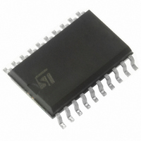
ST72F623F2M1 STMicroelectronics, ST72F623F2M1 Datasheet - Page 32

ST72F623F2M1
Manufacturer Part Number
ST72F623F2M1
Description
IC MCU 8BIT LS 8K 20-SOIC
Manufacturer
STMicroelectronics
Series
ST7r
Datasheet
1.ST72F622L2M1.pdf
(139 pages)
Specifications of ST72F623F2M1
Core Processor
ST7
Core Size
8-Bit
Speed
8MHz
Connectivity
USB
Peripherals
DMA, LVD, POR, PWM, WDT
Number Of I /o
11
Program Memory Size
8KB (8K x 8)
Program Memory Type
FLASH
Ram Size
384 x 8
Voltage - Supply (vcc/vdd)
4 V ~ 5.5 V
Data Converters
A/D 3x10b
Oscillator Type
Internal
Operating Temperature
0°C ~ 70°C
Package / Case
20-SOIC (7.5mm Width)
Processor Series
ST72F6x
Core
ST7
Data Bus Width
8 bit
Data Ram Size
384 B
Interface Type
SCI, SPI, USB
Maximum Clock Frequency
12 MHz
Number Of Programmable I/os
11
Number Of Timers
2
Operating Supply Voltage
4 V to 5.5 V
Maximum Operating Temperature
+ 70 C
Mounting Style
SMD/SMT
Minimum Operating Temperature
0 C
On-chip Adc
10 bit
Lead Free Status / RoHS Status
Contains lead / RoHS non-compliant
Eeprom Size
-
Lead Free Status / Rohs Status
Details
Other names
497-2114-5
Available stocks
Company
Part Number
Manufacturer
Quantity
Price
Company:
Part Number:
ST72F623F2M1
Manufacturer:
NXP
Quantity:
670
Part Number:
ST72F623F2M1
Manufacturer:
ST
Quantity:
20 000
ST7262xxx
9 I/O PORTS
9.1 INTRODUCTION
The I/O ports offer different functional modes:
transfer of data through digital inputs and outputs
and for specific pins:
– Analog signal input (ADC)
– Alternate signal input/output for the on-chip pe-
– External interrupt generation
An I/O port is composed of up to 8 pins. Each pin
can be programmed independently as digital input
or digital output.
9.2 FUNCTIONAL DESCRIPTION
Each port is associated with 2 main registers:
– Data Register (DR)
– Data Direction Register (DDR)
Each I/O pin may be programmed using the corre-
sponding register bits in DDR register: bit x corre-
sponding to pin x of the port. The same corre-
spondence is used for the DR register.
Table 8. I/O Pin Functions
9.2.1 Input Modes
The input configuration is selected by clearing the
corresponding DDR register bit.
In this case, reading the DR register returns the
digital value applied to the external I/O pin.
Notes:
1. All the inputs are triggered by a Schmitt trigger.
2. When switching from input mode to output
Interrupt function
When an external interrupt function of an I/O pin, is
enabled using the ITFRE registers, an event on
this I/O can generate an external Interrupt request
to the CPU. The interrupt sensitivity is programma-
32/139
ripherals.
mode, the DR register should be written first to
output the correct value as soon as the port is
configured as an output.
DDR
0
1
MODE
Output
Input
Doc ID 6996 Rev 5
ble, the options are given in the description of the
ITRFRE interrupt registers.
Each pin can independently generate an Interrupt
request.
Each external interrupt vector is linked to a dedi-
cated group of I/O port pins (see Interrupts sec-
tion). If more than one input pin is selected simul-
taneously as interrupt source, this is logically AN-
Ded and inverted. For this reason, if an event oc-
curs on one of the interrupt pins, it masks the other
ones.
9.2.2 Output Mode
The pin is configured in output mode by setting the
corresponding DDR register bit (see Table 7).
In this mode, writing “0” or “1” to the DR register
applies this digital value to the I/O pin through the
latch. Then reading the DR register returns the
previously stored value.
Note: In this mode, the interrupt function is disa-
bled.
9.2.3 Alternate Functions
Digital Alternate Functions
When an on-chip peripheral is configured to use a
pin, the alternate function is automatically select-
ed. This alternate function takes priority over
standard I/O programming. When the signal is
coming from an on-chip peripheral, the I/O pin is
automatically configured in output mode (push-pull
or open drain according to the peripheral).
When the signal is going to an on-chip peripheral,
the I/O pin has to be configured in input mode. In
this case, the pin state is also digitally readable by
addressing the DR register.
Notes:
1. Input pull-up configuration can cause an unex-
2. When the on-chip peripheral uses a pin as input
Warning: Alternate functions of peripherals must
must not be activated when the external interrupts
are enabled on the same pin, in order to avoid
generating spurious interrupts.
pected value at the alternate peripheral input.
and output, this pin must be configured as an
input (DDR = 0).


