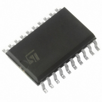
ST72F623F2M1 STMicroelectronics, ST72F623F2M1 Datasheet - Page 78

ST72F623F2M1
Manufacturer Part Number
ST72F623F2M1
Description
IC MCU 8BIT LS 8K 20-SOIC
Manufacturer
STMicroelectronics
Series
ST7r
Datasheet
1.ST72F622L2M1.pdf
(139 pages)
Specifications of ST72F623F2M1
Core Processor
ST7
Core Size
8-Bit
Speed
8MHz
Connectivity
USB
Peripherals
DMA, LVD, POR, PWM, WDT
Number Of I /o
11
Program Memory Size
8KB (8K x 8)
Program Memory Type
FLASH
Ram Size
384 x 8
Voltage - Supply (vcc/vdd)
4 V ~ 5.5 V
Data Converters
A/D 3x10b
Oscillator Type
Internal
Operating Temperature
0°C ~ 70°C
Package / Case
20-SOIC (7.5mm Width)
Processor Series
ST72F6x
Core
ST7
Data Bus Width
8 bit
Data Ram Size
384 B
Interface Type
SCI, SPI, USB
Maximum Clock Frequency
12 MHz
Number Of Programmable I/os
11
Number Of Timers
2
Operating Supply Voltage
4 V to 5.5 V
Maximum Operating Temperature
+ 70 C
Mounting Style
SMD/SMT
Minimum Operating Temperature
0 C
On-chip Adc
10 bit
Lead Free Status / RoHS Status
Contains lead / RoHS non-compliant
Eeprom Size
-
Lead Free Status / Rohs Status
Details
Other names
497-2114-5
Available stocks
Company
Part Number
Manufacturer
Quantity
Price
Company:
Part Number:
ST72F623F2M1
Manufacturer:
NXP
Quantity:
670
Part Number:
ST72F623F2M1
Manufacturer:
ST
Quantity:
20 000
ST7262xxx
SERIAL COMMUNICATIONS INTERFACE (Cont’d)
CONTROL REGISTER 1 (SCICR1)
Read/Write
Reset Value: x000 0000 (x0h)
Bit 7 = R8 Receive data bit 8.
This bit is used to store the 9th bit of the received
word when M = 1.
Bit 6 = T8 Transmit data bit 8.
This bit is used to store the 9th bit of the transmit-
ted word when M = 1.
Bit 5 = SCID Disabled for low power consumption
When this bit is set the SCI prescalers and outputs
are stopped and the end of the current byte trans-
fer in order to reduce power consumption.This bit
is set and cleared by software.
0: SCI enabled
1: SCI prescaler and outputs disabled
Bit 4 = M Word length.
This bit determines the word length. It is set or
cleared by software.
0: 1 Start bit, 8 Data bits, 1 Stop bit
1: 1 Start bit, 9 Data bits, 1 Stop bit
Note: The M bit must not be modified during a data
transfer (both transmission and reception).
78/139
R8
7
T8
SCID
M
WAKE
PCE
PS
PIE
0
Doc ID 6996 Rev 5
Bit 3 = WAKE Wake-Up method.
This bit determines the SCI Wake-Up method, it is
set or cleared by software.
0: Idle Line
1: Address Mark
Bit 2 = PCE Parity control enable.
This bit selects the hardware parity control (gener-
ation and detection). When the parity control is en-
abled, the computed parity is inserted at the MSB
position (9th bit if M = 1; 8th bit if M = 0) and parity
is checked on the received data. This bit is set and
cleared by software. Once it is set, PCE is active
after the current byte (in reception and in transmis-
sion).
0: Parity control disabled
1: Parity control enabled
Bit 1 = PS Parity selection.
This bit selects the odd or even parity when the
parity generation/detection is enabled (PCE bit
set). It is set and cleared by software. The parity is
selected after the current byte.
0: Even parity
1: Odd parity
Bit 0 = PIE Parity interrupt enable.
This bit enables the interrupt capability of the hard-
ware parity control when a parity error is detected
(PE bit set). It is set and cleared by software.
0: Parity error interrupt disabled
1: Parity error interrupt enabled.


