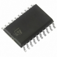
ST72F623F2M1 STMicroelectronics, ST72F623F2M1 Datasheet - Page 120

ST72F623F2M1
Manufacturer Part Number
ST72F623F2M1
Description
IC MCU 8BIT LS 8K 20-SOIC
Manufacturer
STMicroelectronics
Series
ST7r
Datasheet
1.ST72F622L2M1.pdf
(139 pages)
Specifications of ST72F623F2M1
Core Processor
ST7
Core Size
8-Bit
Speed
8MHz
Connectivity
USB
Peripherals
DMA, LVD, POR, PWM, WDT
Number Of I /o
11
Program Memory Size
8KB (8K x 8)
Program Memory Type
FLASH
Ram Size
384 x 8
Voltage - Supply (vcc/vdd)
4 V ~ 5.5 V
Data Converters
A/D 3x10b
Oscillator Type
Internal
Operating Temperature
0°C ~ 70°C
Package / Case
20-SOIC (7.5mm Width)
Processor Series
ST72F6x
Core
ST7
Data Bus Width
8 bit
Data Ram Size
384 B
Interface Type
SCI, SPI, USB
Maximum Clock Frequency
12 MHz
Number Of Programmable I/os
11
Number Of Timers
2
Operating Supply Voltage
4 V to 5.5 V
Maximum Operating Temperature
+ 70 C
Mounting Style
SMD/SMT
Minimum Operating Temperature
0 C
On-chip Adc
10 bit
Lead Free Status / RoHS Status
Contains lead / RoHS non-compliant
Eeprom Size
-
Lead Free Status / Rohs Status
Details
Other names
497-2114-5
Available stocks
Company
Part Number
Manufacturer
Quantity
Price
Company:
Part Number:
ST72F623F2M1
Manufacturer:
NXP
Quantity:
670
Part Number:
ST72F623F2M1
Manufacturer:
ST
Quantity:
20 000
12.12 10-BIT ADC CHARACTERISTICS
Subject to general operating conditions for V
Figure 81. R
Figure 83. Typical Application with ADC
Notes:
1. Unless otherwise specified, typical data are based on T
lines and are not tested.
2. When V
3. Any added external serial resistor will downgrade the ADC accuracy (especially for resistance greater than 10kΩ). Data
based on characterization results, not tested in production.
4. C
pacitance (3pF). A high C
5. This graph shows that depending on the input signal variation (f
the use of a larger serial resistor (R
6. Please refer to Important Notes on conversion speed,
silicon revision identification.
120/139
Symbol
t
CONV
C
R
C
f
V
f
45
40
35
30
25
20
15
10
ADC
AIN
PARASITIC
ADC
5
0
AIN
AIN
AIN
6)
DDA
0
ADC clock frequency
Conversion voltage range
External input impedance
External capacitor on analog input
Variation frequency of analog input signal
Internal sample and hold capacitor
Conversion time
Flash silicon rev. G devices
Conversion time
Flash silicon rev. X and ROM rev. Z devices
V
AIN
represents the capacitance of the PCB (dependent on soldering and PCB layout quality) plus the pad ca-
AIN
and V
max. vs f
10
SSA
C
PARASITIC
R
pins are not available on the pinout, the ADC refers to V
AIN
PARASITIC
(pF)
Parameter
ADC
30
C
AIN
with C
AIN)
value will downgrade conversion accuracy. To remedy this, f
2)
4 MHz
2 MHz
1 MHz
. It is valid for all f
AINx
70
AIN
=0pF
DD,
4)
f
CPU
ADC
Doc ID 6996 Rev 5
A
Section 15.2
=25°C and V
V
, and T
f
frequencies ≤ 4MHz.
DD
ADC
Conditions
Figure 82. Recommended C
V
0.6V
V
0.6V
AIN
=4MHz
T
T
1000
100
0.1
10
), C
1
A
unless otherwise specified
and also to
DD
AIN
-V
0.01
can be increased for stabilization and to allow
SS
2kΩ(max)
=5V. They are given only as design guide-
I
±1μA
L
V
Min
0.4
DD
SSA
Figure 92. on page 137
0.1
and V
f
AIN
(KHz)
Typ
SS
10-Bit A/D
Conversion
112
16
28
6
.
4
1)
1
ADC
AIN
Cain 10 nF
Cain 22 nF
Cain 47 nF
Figure 81
82
/R
Figure
should be reduced.
V
Max
see
and
3)4)5)
AIN
DDA
4
10
ST72XXX
for details on
values
C
6pF
ADC
1/f
1/f
Unit
MHz
kΩ
Hz
pF
pF
μs
μs
V
ADC
ADC
5)


