M30873FHBGP#U3 Renesas Electronics America, M30873FHBGP#U3 Datasheet - Page 95
M30873FHBGP#U3
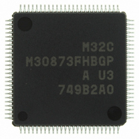
Manufacturer Part Number
M30873FHBGP#U3
Description
IC M32C/87 MCU FLASH 100LQFP
Manufacturer
Renesas Electronics America
Series
M16C™ M32C/80r
Datasheet
1.M3087BFLGPU3.pdf
(629 pages)
Specifications of M30873FHBGP#U3
Core Processor
M32C/80
Core Size
16/32-Bit
Speed
32MHz
Connectivity
EBI/EMI, I²C, IEBus, IrDA, SIO, UART/USART
Peripherals
DMA, POR, PWM, WDT
Number Of I /o
85
Program Memory Size
384KB (384K x 8)
Program Memory Type
FLASH
Ram Size
24K x 8
Voltage - Supply (vcc/vdd)
3 V ~ 5.5 V
Data Converters
A/D 26x10b; D/A 2x8b
Oscillator Type
Internal
Operating Temperature
-40°C ~ 85°C
Package / Case
100-LQFP
For Use With
R0K330879S001BE - KIT DEV RSK M32C/87R0K330879S000BE - KIT DEV RSK M32C/87
Lead Free Status / RoHS Status
Lead free / RoHS Compliant
Eeprom Size
-
Available stocks
Company
Part Number
Manufacturer
Quantity
Price


M32C/87 Group (M32C/87, M32C/87A, M32C/87B)
REJ09B0180-0151 Rev.1.51 Jul 31, 2008
Page 71 of 587
Figure 8.4
• Bus cycle 1 φ + 1 φ
• Bus cycle 1 φ + 3 φ
• Bus cycle 1 φ + 5 φ
WR, WRL, WRH
WR, WRL, WRH
WR, WRL, WRH
Read data
Write data
Read data
Write data
Read data
Write data
Address
Address
Address
NOTE:
i = 0 to 3
BCLK
BCLK
BCLK
1. When the MCU accesses the same CS area consecutively, the
CSi
CSi
RD
CSi
RD
RD
1 bus cycle = 2
1 bus cycle = 4
Bus Cycles when Separate Bus is Selected (1/3)
1 bus cycle = 6
φ
φ
(Note 1)
φ
(Note 1)
(Note 1)
• Bus cycle 1 φ + 4 φ
• Bus cycle 1 φ + 6 φ
• Bus cycle 1 φ + 2 φ
WR, WRL, WRH
WR, WRL, WRH
WR, WRL, WRH
Read data
Read data
Read data
Write data
Write data
Write data
CSi
Address
Address
Address
BCLK
BCLK
BCLK
pin keeps outputting "L".
CSi
CSi
CSi
RD
RD
RD
1 bus cycle = 3
1 bus cycle = 5
1 bus cycle = 7
φ
φ
φ
(Note 1)
(Note 1)
(Note 1)
8. Bus
Related parts for M30873FHBGP#U3
Image
Part Number
Description
Manufacturer
Datasheet
Request
R

Part Number:
Description:
KIT STARTER FOR M16C/29
Manufacturer:
Renesas Electronics America
Datasheet:

Part Number:
Description:
KIT STARTER FOR R8C/2D
Manufacturer:
Renesas Electronics America
Datasheet:

Part Number:
Description:
R0K33062P STARTER KIT
Manufacturer:
Renesas Electronics America
Datasheet:

Part Number:
Description:
KIT STARTER FOR R8C/23 E8A
Manufacturer:
Renesas Electronics America
Datasheet:

Part Number:
Description:
KIT STARTER FOR R8C/25
Manufacturer:
Renesas Electronics America
Datasheet:

Part Number:
Description:
KIT STARTER H8S2456 SHARPE DSPLY
Manufacturer:
Renesas Electronics America
Datasheet:

Part Number:
Description:
KIT STARTER FOR R8C38C
Manufacturer:
Renesas Electronics America
Datasheet:

Part Number:
Description:
KIT STARTER FOR R8C35C
Manufacturer:
Renesas Electronics America
Datasheet:

Part Number:
Description:
KIT STARTER FOR R8CL3AC+LCD APPS
Manufacturer:
Renesas Electronics America
Datasheet:
Part Number:
Description:
KIT STARTER FOR RX610
Manufacturer:
Renesas Electronics America
Datasheet:

Part Number:
Description:
KIT STARTER FOR R32C/118
Manufacturer:
Renesas Electronics America
Datasheet:

Part Number:
Description:
KIT DEV RSK-R8C/26-29
Manufacturer:
Renesas Electronics America
Datasheet:

Part Number:
Description:
KIT STARTER FOR SH7124
Manufacturer:
Renesas Electronics America
Datasheet:

Part Number:
Description:
KIT STARTER FOR H8SX/1622
Manufacturer:
Renesas Electronics America
Datasheet:

Part Number:
Description:
KIT DEV FOR SH7203
Manufacturer:
Renesas Electronics America
Datasheet: