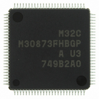
M30873FHBGP#U3 Renesas Electronics America, M30873FHBGP#U3 Datasheet - Page 349

M30873FHBGP#U3
Manufacturer Part Number
M30873FHBGP#U3
Description
IC M32C/87 MCU FLASH 100LQFP
Manufacturer
Renesas Electronics America
Series
M16C™ M32C/80r
Datasheet
1.M3087BFLGPU3.pdf
(629 pages)
Specifications of M30873FHBGP#U3
Core Processor
M32C/80
Core Size
16/32-Bit
Speed
32MHz
Connectivity
EBI/EMI, I²C, IEBus, IrDA, SIO, UART/USART
Peripherals
DMA, POR, PWM, WDT
Number Of I /o
85
Program Memory Size
384KB (384K x 8)
Program Memory Type
FLASH
Ram Size
24K x 8
Voltage - Supply (vcc/vdd)
3 V ~ 5.5 V
Data Converters
A/D 26x10b; D/A 2x8b
Oscillator Type
Internal
Operating Temperature
-40°C ~ 85°C
Package / Case
100-LQFP
For Use With
R0K330879S001BE - KIT DEV RSK M32C/87R0K330879S000BE - KIT DEV RSK M32C/87
Lead Free Status / RoHS Status
Lead free / RoHS Compliant
Eeprom Size
-
Available stocks
Company
Part Number
Manufacturer
Quantity
Price
- Current page: 349 of 629
- Download datasheet (16Mb)
M32C/87 Group (M32C/87, M32C/87A, M32C/87B)
REJ09B0180-0151 Rev.1.51 Jul 31, 2008
Page 325 of 587
Figure 22.4
Group 1 Base Timer Control Register 1
b7
b6 b5 b4
NOTES:
1. The base timer is reset at the second fBT1 clock cycle after the base timer matches the G1PO0 register.
2. The IPSA_0 bit in the IPSA register selects the input pin, either INT0 or INT1.
3. Use the BTSR register when multiple base timers start counting simultaneously. In this case, set the BTS bit to 0.
4. In two-phase pulse signal processing mode, the base timer is not reset if the counter is decremented at the second clock cycle
after the base timer matches the G1PO0 register, even though the RST1 bit is set to 1.
b3
0
b2
G1BCR1 Register
b1
b0
Bit Symbol
RST1
RST2
BTS
UD0
UD1
(b0)
(b3)
(b7)
Symbol
G1BCR1
−
−
−
Unimplemented.
Write 0. Read as undefined value.
Base timer reset source
select bit 1
Base timer reset source
select bit 2
Reserved bit
Base timer start bit
Counter increment/
decrement control bits
Unimplemented.
Write 0. Read as undefined value.
Bit Name
(3)
Address
0123h
0: Base timer is not reset by applying "L" to the
1: Base timer is reset by applying "L" to the INT0
0: Base timer is not reset by matching
1: Base timer is reset by matching
Set to 0
0: Base timer reset
1: Base timer count starts
b6 b5
0 0: Counter increment mode
0 1: Counter increment/decrement mode
1 0: Two-phase pulse signal processing mode
1 1: Do not set to this value
the G1PO0 register
the G1PO0 register
INT0 or INT1 pin
or INT1 pin
(2)
Function
(1)
After Reset
X000 000Xb
(4)
22. Intelligent I/O
RW
RW
RW
RW
RW
RW
RW
−
−
Related parts for M30873FHBGP#U3
Image
Part Number
Description
Manufacturer
Datasheet
Request
R

Part Number:
Description:
KIT STARTER FOR M16C/29
Manufacturer:
Renesas Electronics America
Datasheet:

Part Number:
Description:
KIT STARTER FOR R8C/2D
Manufacturer:
Renesas Electronics America
Datasheet:

Part Number:
Description:
R0K33062P STARTER KIT
Manufacturer:
Renesas Electronics America
Datasheet:

Part Number:
Description:
KIT STARTER FOR R8C/23 E8A
Manufacturer:
Renesas Electronics America
Datasheet:

Part Number:
Description:
KIT STARTER FOR R8C/25
Manufacturer:
Renesas Electronics America
Datasheet:

Part Number:
Description:
KIT STARTER H8S2456 SHARPE DSPLY
Manufacturer:
Renesas Electronics America
Datasheet:

Part Number:
Description:
KIT STARTER FOR R8C38C
Manufacturer:
Renesas Electronics America
Datasheet:

Part Number:
Description:
KIT STARTER FOR R8C35C
Manufacturer:
Renesas Electronics America
Datasheet:

Part Number:
Description:
KIT STARTER FOR R8CL3AC+LCD APPS
Manufacturer:
Renesas Electronics America
Datasheet:

Part Number:
Description:
KIT STARTER FOR RX610
Manufacturer:
Renesas Electronics America
Datasheet:

Part Number:
Description:
KIT STARTER FOR R32C/118
Manufacturer:
Renesas Electronics America
Datasheet:

Part Number:
Description:
KIT DEV RSK-R8C/26-29
Manufacturer:
Renesas Electronics America
Datasheet:

Part Number:
Description:
KIT STARTER FOR SH7124
Manufacturer:
Renesas Electronics America
Datasheet:

Part Number:
Description:
KIT STARTER FOR H8SX/1622
Manufacturer:
Renesas Electronics America
Datasheet:

Part Number:
Description:
KIT DEV FOR SH7203
Manufacturer:
Renesas Electronics America
Datasheet:


