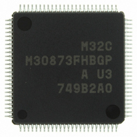
M30873FHBGP#U3 Renesas Electronics America, M30873FHBGP#U3 Datasheet - Page 369

M30873FHBGP#U3
Manufacturer Part Number
M30873FHBGP#U3
Description
IC M32C/87 MCU FLASH 100LQFP
Manufacturer
Renesas Electronics America
Series
M16C™ M32C/80r
Datasheet
1.M3087BFLGPU3.pdf
(629 pages)
Specifications of M30873FHBGP#U3
Core Processor
M32C/80
Core Size
16/32-Bit
Speed
32MHz
Connectivity
EBI/EMI, I²C, IEBus, IrDA, SIO, UART/USART
Peripherals
DMA, POR, PWM, WDT
Number Of I /o
85
Program Memory Size
384KB (384K x 8)
Program Memory Type
FLASH
Ram Size
24K x 8
Voltage - Supply (vcc/vdd)
3 V ~ 5.5 V
Data Converters
A/D 26x10b; D/A 2x8b
Oscillator Type
Internal
Operating Temperature
-40°C ~ 85°C
Package / Case
100-LQFP
For Use With
R0K330879S001BE - KIT DEV RSK M32C/87R0K330879S000BE - KIT DEV RSK M32C/87
Lead Free Status / RoHS Status
Lead free / RoHS Compliant
Eeprom Size
-
Available stocks
Company
Part Number
Manufacturer
Quantity
Price
- Current page: 369 of 629
- Download datasheet (16Mb)
M32C/87 Group (M32C/87, M32C/87A, M32C/87B)
REJ09B0180-0151 Rev.1.51 Jul 31, 2008
Page 345 of 587
Figure 22.20
(1) When digital filter function is not used (Bits DF1 and DF0 in the G1TMCRi register are set to 00b)
(2) When digital filter function is used (Bits DF1 and DF0 in the G1TMCRi register are set to 10b
Internal trigger signal
Input to
the INPC1_i pin
Internal trigger signal
Base timer 1
Count source of
base timer
Base timer value
Read value from the
G1BT register
G1TMi register
TM1iR bit
(fBT1 is selected as sampling clock))
Input to
the INPC1_i pin
Count source of
base timer
Base timer value
G1TMi register
TM1iR bit
i = 0 to 7
The TM1iR bit: bit in registers IIO0IR to IIO4IR and IIO8IR to IIO10IR
The above applies under the following conditions:
- G1TMCRi register: bits CTS1 and CTS0 are set to 01b (rising edge is selected for time measurement trigger)
- G1BCR1 register:
NOTE:
1. The width of pulse input to INPC1_i pin requires 1.5 or more fBT1 clock cycles.
Time Measurement Function Operation
FFFFh
0000h
"H"
"H"
"H"
"H"
"L"
"L"
"L"
"L"
1
0
1
0
the PR bit is set to 0 (prescaler function is not used)
the GT bit is set to 0 (gate function is not used)
bits RST2 and RST1 are set to 00b (base timer is not reset)
bits UD1 and UD0 are set to 00b (counter increment mode)
m-1
m
m
m
(Note 1)
m+1
m+1
m+1
m+2
m+2
An input signal which does not match its
level three times is ignored
m+2
m+3
m+3
Set to 0 by a program
m+3
m+4
m+4
m+1
m+4
m+5
m+5
Max. of 1.5 clock cycles delay
m+5
m+6
m+6
Trigger signal is delayed for max. 4.5 clock cycles
due to the digital filter
m+6
m+7
m+7
22. Intelligent I/O (Time Measurement Function)
m+7
m+8
m+8
m+8
m+9
m+9
m+9
m+10 m+11 m+12 m+13
m+10 m+11 m+12 m+13
m+10 m+11 m+12 m+13
m+7
Set to 0 by a program
m+10
FFFF
FFFF
FFFF
Related parts for M30873FHBGP#U3
Image
Part Number
Description
Manufacturer
Datasheet
Request
R

Part Number:
Description:
KIT STARTER FOR M16C/29
Manufacturer:
Renesas Electronics America
Datasheet:

Part Number:
Description:
KIT STARTER FOR R8C/2D
Manufacturer:
Renesas Electronics America
Datasheet:

Part Number:
Description:
R0K33062P STARTER KIT
Manufacturer:
Renesas Electronics America
Datasheet:

Part Number:
Description:
KIT STARTER FOR R8C/23 E8A
Manufacturer:
Renesas Electronics America
Datasheet:

Part Number:
Description:
KIT STARTER FOR R8C/25
Manufacturer:
Renesas Electronics America
Datasheet:

Part Number:
Description:
KIT STARTER H8S2456 SHARPE DSPLY
Manufacturer:
Renesas Electronics America
Datasheet:

Part Number:
Description:
KIT STARTER FOR R8C38C
Manufacturer:
Renesas Electronics America
Datasheet:

Part Number:
Description:
KIT STARTER FOR R8C35C
Manufacturer:
Renesas Electronics America
Datasheet:

Part Number:
Description:
KIT STARTER FOR R8CL3AC+LCD APPS
Manufacturer:
Renesas Electronics America
Datasheet:

Part Number:
Description:
KIT STARTER FOR RX610
Manufacturer:
Renesas Electronics America
Datasheet:

Part Number:
Description:
KIT STARTER FOR R32C/118
Manufacturer:
Renesas Electronics America
Datasheet:

Part Number:
Description:
KIT DEV RSK-R8C/26-29
Manufacturer:
Renesas Electronics America
Datasheet:

Part Number:
Description:
KIT STARTER FOR SH7124
Manufacturer:
Renesas Electronics America
Datasheet:

Part Number:
Description:
KIT STARTER FOR H8SX/1622
Manufacturer:
Renesas Electronics America
Datasheet:

Part Number:
Description:
KIT DEV FOR SH7203
Manufacturer:
Renesas Electronics America
Datasheet:


