M30873FHBGP#U3 Renesas Electronics America, M30873FHBGP#U3 Datasheet - Page 383
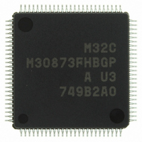
M30873FHBGP#U3
Manufacturer Part Number
M30873FHBGP#U3
Description
IC M32C/87 MCU FLASH 100LQFP
Manufacturer
Renesas Electronics America
Series
M16C™ M32C/80r
Datasheet
1.M3087BFLGPU3.pdf
(629 pages)
Specifications of M30873FHBGP#U3
Core Processor
M32C/80
Core Size
16/32-Bit
Speed
32MHz
Connectivity
EBI/EMI, I²C, IEBus, IrDA, SIO, UART/USART
Peripherals
DMA, POR, PWM, WDT
Number Of I /o
85
Program Memory Size
384KB (384K x 8)
Program Memory Type
FLASH
Ram Size
24K x 8
Voltage - Supply (vcc/vdd)
3 V ~ 5.5 V
Data Converters
A/D 26x10b; D/A 2x8b
Oscillator Type
Internal
Operating Temperature
-40°C ~ 85°C
Package / Case
100-LQFP
For Use With
R0K330879S001BE - KIT DEV RSK M32C/87R0K330879S000BE - KIT DEV RSK M32C/87
Lead Free Status / RoHS Status
Lead free / RoHS Compliant
Eeprom Size
-
Available stocks
Company
Part Number
Manufacturer
Quantity
Price


M32C/87 Group (M32C/87, M32C/87A, M32C/87B)
REJ09B0180-0151 Rev.1.51 Jul 31, 2008
Page 359 of 587
Figure 22.29
(1) When the base timer is not reset
i = 1, 2; j = 0, 2, 4, 6; k = j + 1
m: Setting value of the GiPOj register (0000h to FFFFh), n: Setting value of the GiPOk register (0000h to FFFFh)
The above applies under the following conditions:
- Group 1: In the G1BCR1 register, bits RST2 and RST1 bit are set to 00b and bits UD1 and UD0 are set to 00b (counter increment mode)
- Group 2: Bits RST2 to RST0 in the G2BCR1 register are set to 000b (base timer is not reset by matching the G2PO0 register)
- In the GiPOCRj register, the IVL bit is set to 0 ("L" output) and the INV bit is set to 0 (output not inverted)
- m < n
(2) When the base timer is reset by matching the GiPO0 register
Base timer i
Count source of
base timer
Base timer value
Read value from
the GiBT register
OUTCi_j pin
POijR bit
in the IIOqIR register
POikR bit
in the IIOqIR register
Base timer i
Count source of
base timer
Base timer value
Read value from
the GiBT register
OUTCi_j pin
POijR bit
in the IIOqIR register
POikR bit
in the IIOqIR register
(q = 1 to 3, 6, 7, 9 to 11)
(q = 0, 3 to 5, 8 to 10)
(q = 1, 2, 7, 9 to 11)
(q = 0, 3, 4, 8 to 10)
i = 1, 2; j = 2, 4, 6; k = j + 1
m: Setting value of the GiPOj register (0000h to FFFFh), n: Setting value of the GiPOk register (0000h to FFFFh)
p: Setting value of the GiPO0 register (0001h to FFFDh)
The above applies under the following conditions:
- Group 1: In the G1BCR1 register, bits RST2 and RST1 are set to 01b and bits UD1 and UD0 are set to 00b (counter increment mode)
- Group 2: Bits RST2 to RST0 in the G2BCR1 register are set to 010b (base timer is reset by matching the G2PO0 register)
- In the GiPOCRj register, the IVL bit is set to 0 ("L" output) and the INV bit is set to 0 (output not inverted)
- m < n < p + 2
SR Waveform Output Mode Operation
FFFFh
0000h
0000h
"H"
p+1
"H"
"L"
"L"
m
m
n
1
0
1
0
1
0
1
0
n
m-1
m-1
m-1
m-1
Match
Match
m
m
m
m
m+1
m+1
m+1
m+1
m+2
m+2
m+2
m+2
n - m
n - m
fBTi
fBTi
Match
Match
n
n
n
n
Set to 0 by a program
Set to 0 by a program
n+1
n+1
22. Intelligent I/O (Waveform Generation Function)
n+1
n+1
n+2
n+2
p
p
FFFF 0000
p+1
65536 - n + m
FFFF 0000
p+1
P + 2 - n + m
Reset
fBTi
0000
Set to 0 by a program
fBTi
Set to 0 by a program
0000
Match
Match
m
m
m
m
m+1
m+1
m+1
m+1
m+2
m+2
m+2
m+2
Related parts for M30873FHBGP#U3
Image
Part Number
Description
Manufacturer
Datasheet
Request
R

Part Number:
Description:
KIT STARTER FOR M16C/29
Manufacturer:
Renesas Electronics America
Datasheet:

Part Number:
Description:
KIT STARTER FOR R8C/2D
Manufacturer:
Renesas Electronics America
Datasheet:

Part Number:
Description:
R0K33062P STARTER KIT
Manufacturer:
Renesas Electronics America
Datasheet:

Part Number:
Description:
KIT STARTER FOR R8C/23 E8A
Manufacturer:
Renesas Electronics America
Datasheet:

Part Number:
Description:
KIT STARTER FOR R8C/25
Manufacturer:
Renesas Electronics America
Datasheet:

Part Number:
Description:
KIT STARTER H8S2456 SHARPE DSPLY
Manufacturer:
Renesas Electronics America
Datasheet:

Part Number:
Description:
KIT STARTER FOR R8C38C
Manufacturer:
Renesas Electronics America
Datasheet:

Part Number:
Description:
KIT STARTER FOR R8C35C
Manufacturer:
Renesas Electronics America
Datasheet:

Part Number:
Description:
KIT STARTER FOR R8CL3AC+LCD APPS
Manufacturer:
Renesas Electronics America
Datasheet:
Part Number:
Description:
KIT STARTER FOR RX610
Manufacturer:
Renesas Electronics America
Datasheet:

Part Number:
Description:
KIT STARTER FOR R32C/118
Manufacturer:
Renesas Electronics America
Datasheet:

Part Number:
Description:
KIT DEV RSK-R8C/26-29
Manufacturer:
Renesas Electronics America
Datasheet:

Part Number:
Description:
KIT STARTER FOR SH7124
Manufacturer:
Renesas Electronics America
Datasheet:

Part Number:
Description:
KIT STARTER FOR H8SX/1622
Manufacturer:
Renesas Electronics America
Datasheet:

Part Number:
Description:
KIT DEV FOR SH7203
Manufacturer:
Renesas Electronics America
Datasheet: