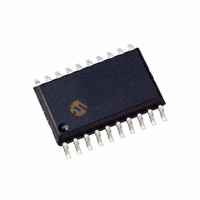
PIC16F785-I/SO Microchip Technology, PIC16F785-I/SO Datasheet - Page 82

PIC16F785-I/SO
Manufacturer Part Number
PIC16F785-I/SO
Description
IC PIC MCU FLASH 2KX14 20SOIC
Manufacturer
Microchip Technology
Series
PIC® 16Fr
Datasheets
1.PIC16F616T-ISL.pdf
(8 pages)
2.PIC16F785-ISS.pdf
(206 pages)
3.PIC16F785-ISS.pdf
(10 pages)
4.PIC16F785-ISS.pdf
(28 pages)
5.PIC16F785-IP.pdf
(178 pages)
Specifications of PIC16F785-I/SO
Program Memory Type
FLASH
Program Memory Size
3.5KB (2K x 14)
Package / Case
20-SOIC (7.5mm Width)
Core Processor
PIC
Core Size
8-Bit
Speed
20MHz
Peripherals
Brown-out Detect/Reset, POR, PWM, WDT
Number Of I /o
17
Eeprom Size
256 x 8
Ram Size
128 x 8
Voltage - Supply (vcc/vdd)
2 V ~ 5.5 V
Data Converters
A/D 14x10b
Oscillator Type
Internal
Operating Temperature
-40°C ~ 85°C
Processor Series
PIC16F
Core
PIC
Data Bus Width
8 bit
Data Ram Size
128 B
Interface Type
RS- 232/USB
Maximum Clock Frequency
20 MHz
Number Of Programmable I/os
17
Number Of Timers
3
Operating Supply Voltage
2 V to 5.5 V
Maximum Operating Temperature
+ 85 C
Mounting Style
SMD/SMT
3rd Party Development Tools
52715-96, 52716-328, 52717-734
Development Tools By Supplier
PG164130, DV164035, DV244005, DV164005, PG164120, ICE2000, DV164120, DM163029
Minimum Operating Temperature
- 40 C
On-chip Adc
14-ch x 10-bit
Lead Free Status / RoHS Status
Lead free / RoHS Compliant
For Use With
XLT20SO1-1 - SOCKET TRANS ICE 20DIP TO 20SOICXLT18SO-1 - SOCKET TRANSITION 18SOIC 300MILAC162060 - HEADER INTRFC MPLAB ICD2 20PINAC164039 - MODULE SKT PROMATE II 20DIP/SOIC
Connectivity
-
Lead Free Status / Rohs Status
Lead free / RoHS Compliant
Available stocks
Company
Part Number
Manufacturer
Quantity
Price
Part Number:
PIC16F785-I/SO
Manufacturer:
MICROCHIP/微芯
Quantity:
20 000
PIC16F785/HV785
12.1
There are four registers available to control the
functionality of the A/D module:
1.
2.
3.
4.
12.1.1
The ANS<11:0> bits, of the ANSEL1 and ANSEL0
Registers, and the TRISA<4,2:0>, TRISB<5:4> and
TRISC<7:6,3:0>> bits control the operation of the A/D
port pins. Set the corresponding TRISx bits to ‘1’ to set
the pin output driver to its high-impedance state. Like-
wise, set the corresponding ANSx bit to disable the dig-
ital input buffer.
12.1.2
There are fourteen analog channels on the PIC16F785/
HV785. The CHS<3:0> bits of the ADCON0 Register
control which channel is connected to the sample and
hold circuit.
TABLE 12-1:
DS41249E-page 80
Legend: Shaded cells are outside of recommended range.
Note 1:
Note:
Operation
16 T
32 T
64 T
A/D RC
ANSEL0 (Register 12-1)
ANSEL1 (Register 12-2)
ADCON0 (Register 12-3)
ADCON1 (Register 12-4)
2 T
4 T
8 T
A/D Clock Source (T
2:
3:
4:
OSC
OSC
OSC
OSC
OSC
OSC
A/D Configuration and Operation
The A/D RC source has a typical T
These values violate the minimum required T
For faster conversion times, the selection of another clock source is recommended.
When the device frequency is greater than 1 MHz, the A/D RC clock source is only recommended if the
conversion will be performed during Sleep.
ANALOG PORT PINS
Analog voltages on any pin that is defined
as a digital input may cause the input
buffer to conduct excess current.
CHANNEL SELECTION
T
ADCS2:ADCS0
AD
VS. DEVICE OPERATING FREQUENCIES
000
100
001
101
010
110
x11
AD
)
2-6 μs
100 ns
200 ns
400 ns
800 ns
20 MHz
1.6 μs
3.2 μs
AD
(1), (4)
(2)
(2)
(2)
(2)
time of 4 μs for V
AD
time.
2-6 μs
12.8 μs
400 ns
800 ns
12.1.3
There are two options for the voltage reference to the
A/D converter: either V
applied to V
Register controls the voltage reference selection. If
VCFG is set, then the voltage on the V
erence; otherwise, V
12.1.4
The A/D conversion cycle requires 11 T
of the conversion clock is software selectable via the
ADCS bits of the ADCON1 Register. There are seven
possible clock options:
• F
• F
• F
• F
• F
• F
• F
For correct conversion, the A/D conversion clock
(1/T
1.6 μs. Table 12-1 shows a few T
selected frequencies.
5 MHz
1.6 μs
3.2 μs
6.4 μs
DD
OSC
OSC
OSC
OSC
OSC
OSC
RC
AD
Device Frequency
(1), (4)
(2)
(2)
(3)
) must be selected to ensure a minimum T
> 3.0V.
(dedicated internal oscillator)
/2
/4
/8
/16
/32
/64
VOLTAGE REFERENCE
REF
CONVERSION CLOCK
is used. The VCFG bit of the ADCON0
2-6 μs
16.0 μs
500 ns
1.0 μs
8.0 μs
DD
4 MHz
2.0 μs
4.0 μs
DD
is the reference.
© 2008 Microchip Technology Inc.
(1), (4)
is used or an analog voltage
(2)
(3)
(2)
(3)
AD
REF
2-6 μs
calculations for
AD
1.25 MHz
12.8 μs
25.6 μs
51.2 μs
1.6 μs
3.2 μs
6.4 μs
pin is the ref-
. The source
(1), (4)
(3)
(3)
(3)
AD
of


