PIC16F785-I/SO Microchip Technology, PIC16F785-I/SO Datasheet - Page 63

PIC16F785-I/SO
Manufacturer Part Number
PIC16F785-I/SO
Description
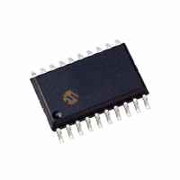
IC PIC MCU FLASH 2KX14 20SOIC
Manufacturer
Microchip Technology
Series
PIC® 16Fr
Datasheets
1.PIC16F616T-ISL.pdf
(8 pages)
2.PIC16F785-ISS.pdf
(206 pages)
3.PIC16F785-ISS.pdf
(10 pages)
4.PIC16F785-ISS.pdf
(28 pages)
5.PIC16F785-IP.pdf
(178 pages)
Specifications of PIC16F785-I/SO
Program Memory Type
FLASH
Program Memory Size
3.5KB (2K x 14)
Package / Case
20-SOIC (7.5mm Width)
Core Processor
PIC
Core Size
8-Bit
Speed
20MHz
Peripherals
Brown-out Detect/Reset, POR, PWM, WDT
Number Of I /o
17
Eeprom Size
256 x 8
Ram Size
128 x 8
Voltage - Supply (vcc/vdd)
2 V ~ 5.5 V
Data Converters
A/D 14x10b
Oscillator Type
Internal
Operating Temperature
-40°C ~ 85°C
Processor Series
PIC16F
Core
PIC
Data Bus Width
8 bit
Data Ram Size
128 B
Interface Type
RS- 232/USB
Maximum Clock Frequency
20 MHz
Number Of Programmable I/os
17
Number Of Timers
3
Operating Supply Voltage
2 V to 5.5 V
Maximum Operating Temperature
+ 85 C
Mounting Style
SMD/SMT
3rd Party Development Tools
52715-96, 52716-328, 52717-734
Development Tools By Supplier
PG164130, DV164035, DV244005, DV164005, PG164120, ICE2000, DV164120, DM163029
Minimum Operating Temperature
- 40 C
On-chip Adc
14-ch x 10-bit
Lead Free Status / RoHS Status
Lead free / RoHS Compliant
For Use With
XLT20SO1-1 - SOCKET TRANS ICE 20DIP TO 20SOICXLT18SO-1 - SOCKET TRANSITION 18SOIC 300MILAC162060 - HEADER INTRFC MPLAB ICD2 20PINAC164039 - MODULE SKT PROMATE II 20DIP/SOIC
Connectivity
-
Lead Free Status / Rohs Status
Lead free / RoHS Compliant
Available stocks
Company
Part Number
Manufacturer
Quantity
Price
Part Number:
PIC16F785-I/SO
Manufacturer:
MICROCHIP/微芯
Quantity:
20 000
8.3.2
The PWM duty cycle is specified by writing to the
CCPR1L register and to the DC1B<1:0> bits of the
CCP1CON register. Up to 10 bits of resolution is avail-
able. The CCPR1L contains the eight MSbs and the
DC1B<1:0> contains the two LSbs. In PWM mode,
CCPR1H is a read-only register.
Equation 8-2 is used to calculate the PWM duty cycle
in time.
EQUATION 8-2:
TABLE 8-3:
© 2008 Microchip Technology Inc.
Timer Prescale (1, 4, 16)
PR2 Value
Maximum Resolution (bits)
PWM duty cycle
Note 1: Changing duty cycle will cause a glitch.
PWM Frequency
PWM DUTY CYCLE
=
EXAMPLE PWM FREQUENCIES AND RESOLUTIONS (F
(
T
CCPR1L:CCP1CON<5:4>
OSC
PWM DUTY CYCLE
• (TMR2 prescale value)
1.22 kHz
0xFF
16
10
(1)
) •
4.88 kHz
0xFF
10
4
(1)
19.53 kHz
CCPR1L and DC1B<1:0> can be written to at any time,
but the duty cycle value is not latched into CCPR1H
until after a match between PR2 and TMR2 occurs
(i.e. the period is complete). In PWM mode, CCPR1H
is a read-only register.
The CCPR1H register and a 2-bit internal latch are
used to double buffer the PWM duty cycle. This double
buffering is essential for glitchless PWM operation.
Because of the buffering, the module waits until the
timer resets, instead of starting immediately. This
means that enhanced PWM waveforms do not exactly
match the standard PWM waveforms, but are instead
offset by one full instruction cycle (4 T
When the CCPR1H and 2-bit latch match TMR2,
concatenated with an internal 2-bit Q clock or 2 bits of
the TMR2 prescaler, the RC5/CCP1 pin is cleared.
The maximum PWM resolution is a function of PR2 as
shown by Equation 8-3.
EQUATION 8-3:
Note:
0xFF
10
1
PIC16F785/HV785
Resolution
If the PWM duty cycle value is longer than
the PWM period, the assigned PWM pin(s)
will remain unchanged.
78.12 kHz
0x3F
1
8
OSC
=
PWM RESOLUTION
log
----------------------------------------- - bits
= 20 MHz)
[
4 PR2
log
156.3 kHz
(
0x1F
2 ( )
1
7
+
DS41249E-page 61
1
OSC
)
]
).
208.3 kHz
0x17
6.6
1


