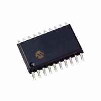
PIC16F785-I/SO Microchip Technology, PIC16F785-I/SO Datasheet - Page 70

PIC16F785-I/SO
Manufacturer Part Number
PIC16F785-I/SO
Description
IC PIC MCU FLASH 2KX14 20SOIC
Manufacturer
Microchip Technology
Series
PIC® 16Fr
Datasheets
1.PIC16F616T-ISL.pdf
(8 pages)
2.PIC16F785-ISS.pdf
(206 pages)
3.PIC16F785-ISS.pdf
(10 pages)
4.PIC16F785-ISS.pdf
(28 pages)
5.PIC16F785-IP.pdf
(178 pages)
Specifications of PIC16F785-I/SO
Program Memory Type
FLASH
Program Memory Size
3.5KB (2K x 14)
Package / Case
20-SOIC (7.5mm Width)
Core Processor
PIC
Core Size
8-Bit
Speed
20MHz
Peripherals
Brown-out Detect/Reset, POR, PWM, WDT
Number Of I /o
17
Eeprom Size
256 x 8
Ram Size
128 x 8
Voltage - Supply (vcc/vdd)
2 V ~ 5.5 V
Data Converters
A/D 14x10b
Oscillator Type
Internal
Operating Temperature
-40°C ~ 85°C
Processor Series
PIC16F
Core
PIC
Data Bus Width
8 bit
Data Ram Size
128 B
Interface Type
RS- 232/USB
Maximum Clock Frequency
20 MHz
Number Of Programmable I/os
17
Number Of Timers
3
Operating Supply Voltage
2 V to 5.5 V
Maximum Operating Temperature
+ 85 C
Mounting Style
SMD/SMT
3rd Party Development Tools
52715-96, 52716-328, 52717-734
Development Tools By Supplier
PG164130, DV164035, DV244005, DV164005, PG164120, ICE2000, DV164120, DM163029
Minimum Operating Temperature
- 40 C
On-chip Adc
14-ch x 10-bit
Lead Free Status / RoHS Status
Lead free / RoHS Compliant
For Use With
XLT20SO1-1 - SOCKET TRANS ICE 20DIP TO 20SOICXLT18SO-1 - SOCKET TRANSITION 18SOIC 300MILAC162060 - HEADER INTRFC MPLAB ICD2 20PINAC164039 - MODULE SKT PROMATE II 20DIP/SOIC
Connectivity
-
Lead Free Status / Rohs Status
Lead free / RoHS Compliant
Available stocks
Company
Part Number
Manufacturer
Quantity
Price
Part Number:
PIC16F785-I/SO
Manufacturer:
MICROCHIP/微芯
Quantity:
20 000
- PIC16F616T-ISL PDF datasheet
- PIC16F785-ISS PDF datasheet #2
- PIC16F785-ISS PDF datasheet #3
- PIC16F785-ISS PDF datasheet #4
- PIC16F785-IP PDF datasheet #5
- Current page: 70 of 206
- Download datasheet (4Mb)
PIC16F785/HV785
9.1.2.2
Comparator C2 has one additional feature: its output
can be synchronized to the Timer1 clock input. Setting
C2SYNC of the CM2CON1 Register synchronizes the
output of Comparator 2 to the falling edge of the Timer1
clock input (see Figure 9-2 and Register 9-3).
The CM2CON1 register also contains mirror copies of
both comparator outputs, MC1OUT and MC2OUT of
the CM2CON1 Register. The ability to read both out-
puts simultaneously from a single register eliminates
the timing skew of reading separate registers.
REGISTER 9-3:
DS41249E-page 68
bit 7
Legend:
R = Readable bit
-n = Value at POR
bit 7
bit 6
bit 5-2
bit 1
bit 0
Note:
MC1OUT
R-0
Obtaining the status of C1OUT or C2OUT
by reading CM2CON1 does not affect the
comparator interrupt mismatch registers.
Control Register CM2CON1
MC1OUT: Mirror Copy of C1OUT bit (CM1CON0<6>)
MC2OUT: Mirror Copy of C2OUT bit (CM2CON0<6>)
Unimplemented: Read as ‘0’
T1GSS: Timer1 Gate Source Select bit
1 = Timer1 gate source is RA4/AN3/T1G/OSC2/CLKOUT
0 = Timer1 gate source is SYNCC2OUT.
C2SYNC: C2 Output Synchronous Mode bit
1 = C2 output is synchronous to falling edge of TMR1 clock
0 = C2 output is asynchronous
MC2OUT
R-0
CM2CON1: COMPARATOR C2 CONTROL REGISTER 1
W = Writable bit
‘1’ = Bit is set
U-0
—
U-0
—
U = Unimplemented bit, read as ‘0’
‘0’ = Bit is cleared
U-0
—
U-0
—
© 2008 Microchip Technology Inc.
x = Bit is unknown
T1GSS
R/W-1
C2SYNC
R/W-0
bit 0
Related parts for PIC16F785-I/SO
Image
Part Number
Description
Manufacturer
Datasheet
Request
R

Part Number:
Description:
IC PIC MCU FLASH 2KX14 20QFN
Manufacturer:
Microchip Technology
Datasheet:

Part Number:
Description:
IC PIC MCU FLASH 2KX14 20DIP
Manufacturer:
Microchip Technology
Datasheet:

Part Number:
Description:
IC PIC MCU FLASH 2KX14 20SSOP
Manufacturer:
Microchip Technology
Datasheet:

Part Number:
Description:
IC PIC MCU FLASH 2KX14 20SOIC
Manufacturer:
Microchip Technology
Datasheet:

Part Number:
Description:
IC PIC MCU FLASH 2KX14 20DIP
Manufacturer:
Microchip Technology
Datasheet:

Part Number:
Description:
3.5 KB Flash, 128 RAM, 18 I/O 20 QFN 4x4mm TUBE
Manufacturer:
Microchip Technology
Datasheet:

Part Number:
Description:
20 PIN, 3.5 KB STD FLASH, 128 RAM, 18 I/O PB FREE,
Manufacturer:
Microchip Technology
Datasheet:

Part Number:
Description:
IC, 8BIT MCU, PIC16F, 32MHZ, SOIC-18
Manufacturer:
Microchip Technology
Datasheet:

Part Number:
Description:
IC, 8BIT MCU, PIC16F, 32MHZ, SSOP-20
Manufacturer:
Microchip Technology
Datasheet:

Part Number:
Description:
IC, 8BIT MCU, PIC16F, 32MHZ, DIP-18
Manufacturer:
Microchip Technology
Datasheet:

Part Number:
Description:
IC, 8BIT MCU, PIC16F, 32MHZ, QFN-28
Manufacturer:
Microchip Technology
Datasheet:

Part Number:
Description:
IC, 8BIT MCU, PIC16F, 32MHZ, QFN-28
Manufacturer:
Microchip Technology
Datasheet:

Part Number:
Description:
IC, 8BIT MCU, PIC16F, 32MHZ, QFN-28
Manufacturer:
Microchip Technology
Datasheet:

Part Number:
Description:
IC, 8BIT MCU, PIC16F, 32MHZ, SSOP-20
Manufacturer:
Microchip Technology
Datasheet:

Part Number:
Description:
IC, 8BIT MCU, PIC16F, 20MHZ, DIP-40
Manufacturer:
Microchip Technology
Datasheet:


