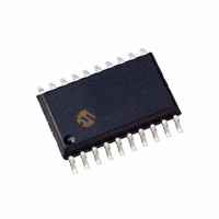
PIC16F785-I/SO Microchip Technology, PIC16F785-I/SO Datasheet - Page 37

PIC16F785-I/SO
Manufacturer Part Number
PIC16F785-I/SO
Description
IC PIC MCU FLASH 2KX14 20SOIC
Manufacturer
Microchip Technology
Series
PIC® 16Fr
Datasheets
1.PIC16F616T-ISL.pdf
(8 pages)
2.PIC16F785-ISS.pdf
(206 pages)
3.PIC16F785-ISS.pdf
(10 pages)
4.PIC16F785-ISS.pdf
(28 pages)
5.PIC16F785-IP.pdf
(178 pages)
Specifications of PIC16F785-I/SO
Program Memory Type
FLASH
Program Memory Size
3.5KB (2K x 14)
Package / Case
20-SOIC (7.5mm Width)
Core Processor
PIC
Core Size
8-Bit
Speed
20MHz
Peripherals
Brown-out Detect/Reset, POR, PWM, WDT
Number Of I /o
17
Eeprom Size
256 x 8
Ram Size
128 x 8
Voltage - Supply (vcc/vdd)
2 V ~ 5.5 V
Data Converters
A/D 14x10b
Oscillator Type
Internal
Operating Temperature
-40°C ~ 85°C
Processor Series
PIC16F
Core
PIC
Data Bus Width
8 bit
Data Ram Size
128 B
Interface Type
RS- 232/USB
Maximum Clock Frequency
20 MHz
Number Of Programmable I/os
17
Number Of Timers
3
Operating Supply Voltage
2 V to 5.5 V
Maximum Operating Temperature
+ 85 C
Mounting Style
SMD/SMT
3rd Party Development Tools
52715-96, 52716-328, 52717-734
Development Tools By Supplier
PG164130, DV164035, DV244005, DV164005, PG164120, ICE2000, DV164120, DM163029
Minimum Operating Temperature
- 40 C
On-chip Adc
14-ch x 10-bit
Lead Free Status / RoHS Status
Lead free / RoHS Compliant
For Use With
XLT20SO1-1 - SOCKET TRANS ICE 20DIP TO 20SOICXLT18SO-1 - SOCKET TRANSITION 18SOIC 300MILAC162060 - HEADER INTRFC MPLAB ICD2 20PINAC164039 - MODULE SKT PROMATE II 20DIP/SOIC
Connectivity
-
Lead Free Status / Rohs Status
Lead free / RoHS Compliant
Available stocks
Company
Part Number
Manufacturer
Quantity
Price
Part Number:
PIC16F785-I/SO
Manufacturer:
MICROCHIP/微芯
Quantity:
20 000
4.0
There are seventeen general purpose I/O pins and one
input only pin available. Depending on which peripher-
als are enabled, some or all of the pins may not be
available as general purpose I/O. In general, when a
peripheral is enabled, the associated pin may not be
used as a general purpose I/O pin.
4.1
PORTA is a 6-bit wide, bidirectional port. The corre-
sponding data direction register is TRISA (Register 4-2).
Setting a TRISA bit (= 1) will make the corresponding
PORTA pin an input (i.e., put the corresponding output
driver in a High-Impedance mode). Clearing a TRISA bit
(= 0) will make the corresponding PORTA pin an output
(i.e., put the contents of the output latch on the selected
pin). The exception is RA3, which is input only and its
TRIS bit will always read as ‘1’. Example 4-1 shows how
to initialize PORTA.
Reading the PORTA register (Register 4-1) reads the
status of the pins, whereas writing to it will write to the
port latch. All write operations are read-modify-write
operations. Therefore, a write to a port implies that the
port pins are read; this value is modified and then
written to the port data latch. RA3 reads ‘0’ when
MCLRE = 1.
REGISTER 4-1:
© 2008 Microchip Technology Inc.
bit 7
Legend:
R = Readable bit
-n = Value at POR
bit 7-6
bit 5-0
Note 1: Data latches are unknown after a POR, but each port bit reads ‘0’ when the corresponding
U-0
—
I/O PORTS
PORTA and TRISA Registers
analog select bit is ‘1’ (see Register 12-1).
Unimplemented: Read as ‘0’
RA<5:0>: PORTA I/O Pin bits
1 = Port pin is greater than V
0 = Port pin is less than V
U-0
—
PORTA: PORTA REGISTER
W = Writable bit
‘1’ = Bit is set
R/W-x
RA5
IL
IH
R/W-x
RA4
(1)
U = Unimplemented bit, read as ‘0’
‘0’ = Bit is cleared
R/W-x
The TRISA register controls the direction of the
PORTA pins, even when they are being used as analog
inputs. The user must ensure the bits in the TRISA
register are maintained set when using them as analog
inputs. I/O pins configured as analog inputs always
read ‘0’.
When RA1 is configured as a voltage reference output,
the RA1 digital output driver will automatically be
disabled while not affecting the TRISA<1> value.
EXAMPLE 4-1:
RA3
BCF
BCF
CLRF
MOVLW
ANDWF
BSF
MOVLW
MOVWF
BCF
Note:
PIC16F785/HV785
STATUS,RP0
STATUS,RP1
PORTA
F8h
ANSEL0,f
STATUS,RP0
0Ch
TRISA
STATUS,RP0
The ANSEL0 (91h) register must be initial-
ized to configure an analog channel as a
digital input. Pins configured as analog
inputs will read ‘0’.
R/W-x
RA2
(1)
INITIALIZING PORTA
;Bank 0
;
;Init PORTA
;Set RA<2:0> to
; digital I/O
;Bank 1
;Set RA<3:2> as inputs
; and set RA<5:4,1:0>
; as outputs
;Bank 0
x = Bit is unknown
R/W-x
RA1
(1)
DS41249E-page 35
R/W-x
RA0
(1)
bit 0


